DATASHEET
5mm Phototransistor
PT1504-6B
Technical Data Sheet
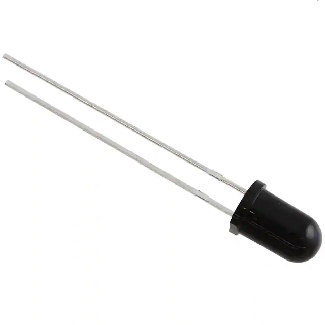
5mm Phototransistor T-1 3/4
Features
․Fast response time
․High photo sensitivity
․Pb free
․This product itself will remain within RoHS compliant version.
․Copliance with EU REACH
․Compliance Halogen Free.(Br<900 ppm,Cl<900ppm,Br+Cl<1500ppm)
Descriptions
․PT1504-6B is a high speed and high sensitive NPN silicon
NPN epitaxial planar phototransistor molded in a standard 5 mm package.
Due to is black epoxy the device is sensitive to visible and near
Infrared radiation.
Applications
․Infrared applied system
․Camera
․Cockroach catcher
Device Selection Guide
1
LED Part No.
Chip
Material
Lens Color
PT1504-6B
Silicon
Black
Copyright © 2010, Everlight All Rights Reserved. Release Date : Dec .09.2016. Issue No: DPT-0000290 _Rev.6
www.everlight.com
�DATASHEET
5mm Phototransistor
PT1504-6B
Package Dimensions
2
2
1
1
2
Emitter
Collector
1
Notes: 1.All dimensions are in millimeters
2.Tolerances unless dimensions ±0.25mm
2
Copyright © 2010, Everlight All Rights Reserved. Release Date : Dec .09.2016. Issue No: DPT-0000290 _Rev.6
www.everlight.com
�DATASHEET
5mm Phototransistor
PT1504-6B
Absolute Maximum Ratings (Ta=25℃)
Parameter
Symbol
Rating
Collector-Emitter Voltage
VCEO
30
Units
V
Emitter-Collector-Voltage
VECO
5
V
IC
mA
Collector Current
Operating Temperature
Topr
20
-25 ~ +85℃
Storage Temperature
Tstg
-40 ~ +85℃
℃
Lead Soldering Temperature(*1)
Tsol
260
℃
Power Dissipation at (or below)
25℃ Free Air Temperature
Pc
75
mW
℃
Notes: *1:Soldering time≦5 seconds.
Electro-Optical Characteristics (Ta=25℃)
Parameter
Collector – Emitter
Breakdown Voltage
3
Symbol
BVCEO
Condition
IC=100μA
Ee=0mW/cm2
Min.
Typ.
Max.
Units
30
---
---
V
Emitter-Collector
Breakdown Voltage
IE=100μA
BVECO Ee=0mW/cm2
5
---
---
V
Collector-Emitter
Saturation Voltage
IC=2mA
VCE)(sat) Ee=1mW/cm2
---
---
0.4
V
---
15
---
---
15
---
---
---
100
nA
1.77
4.0
---
mA
Rise Time
tr
Fall Time
tf
VCE=5V
IC=1mA
RL=1000Ω
Ee=0mW/cm2
VCE=20V
Ee=1mW/cm2
VCE=5V
μS
Collector Dark Current
ICEO
On State Collector Current
IC(on)
Wavelength of
Peak Sensitivity
λp
---
---
940
---
nm
Rang of Spectral Bandwidth
λ0.5
---
---
760-1100
---
nm
Copyright © 2010, Everlight All Rights Reserved. Release Date : Dec .09.2016. Issue No: DPT-0000290 _Rev.6
www.everlight.com
�DATASHEET
5mm Phototransistor
PT1504-6B
Rankings
Parameter
Symbol
Min
Max
Unit
Test Condition
Ic(on)
1.77
2.67
3.61
5.07
mA
4.18
7.07
VcE=5V
Ee=1mW/cm²
J
K
L
Note:
*Measurement Uncertainty of Forward Voltage: ±0.1V
*Measurement Uncertainty of Luminous Intensity: ±10%
*Measurement Uncertainty of Dominant Wavelength ±1.0nm
4
Copyright © 2010, Everlight All Rights Reserved. Release Date : Dec .09.2016. Issue No: DPT-0000290 _Rev.6
www.everlight.com
�DATASHEET
5mm Phototransistor
PT1504-6B
Typical Electro-Optical Characteristics Curves
Fig.1Collector Power Dissipation vs.
Ambient Temperature
160
Fig.2 Spectral Sensitivity
1.0
Ta=25 C
2
140
0.8
120
0.6
100
80
Ambient
Temperature
60
0.4
40
0.2
20
0
0
10
20
30
40 50
60
70
Fig.3 Relative Collector Current vs.
Ambient Temperature
0
700
800
900
1000 1100 1300
Fig.4 Collector Current vs.
Irradiance
100
100
C
80
10
60
1
40
0.1
20
0
-25
0
25
50
75 85 100
0.01
0.5
1
1.5
3
2
5
Copyright © 2010, Everlight All Rights Reserved. Release Date : Dec .09.2016. Issue No: DPT-0000290 _Rev.6
www.everlight.com
�DATASHEET
5mm Phototransistor
PT1504-6B
Typical Electro-Optical Characteristics Curves
Fig.5 Collector Dark Current vs.
Ambient Temperature
Fig.6 Collector Current vs.
Collector-Emitter Voltage
10
14
12
10
10
8
10
6
4
10
2
10
0
6
25
50
75
100
0
0
1
2
Copyright © 2010, Everlight All Rights Reserved. Release Date : Dec .09.2016. Issue No: DPT-0000290 _Rev.6
3
4
www.everlight.com
�DATASHEET
5mm Phototransistor
PT1504-6B
Label Form Specification
CPN: Customer’s Production Number
P/N : Production Number
QTY: Packing Quantity
CAT: Ranks
HUE: Peak Wavelength
REF: Reference
LOT No: Lot Number
Packing Specification
■ Anti-electrostatic bag
■ Inner Carton
■ Outside Carton
■ Packing Quantity
1. MIN 200 To 500PCS/1 Bag, 5 Bags/1 Inner Carton
2. 10 Inner Cartons/1 Outside Carton
Notes
7
Copyright © 2010, Everlight All Rights Reserved. Release Date : Dec .09.2016. Issue No: DPT-0000290 _Rev.6
www.everlight.com
�DATASHEET
5mm Phototransistor
PT1504-6B
1.
Lead Forming
During lead formation, the leads should be bent at a point at least 3mm from the base of the epoxy bulb.
Lead forming should be done before soldering.
Avoid stressing the PHOTOTRANSISTOR package during leads forming. The stress to the base may
damage the PHOTOTRANSISTOR’s characteristics or it may break the Phototransistor.
Cut the PHOTOTRANSISTOR lead frames at room temperature. Cutting the lead frames at high
temperatures may cause failure of the Phototransistor.
When mounting the Phototransistor onto a PCB, the PCB holes must be aligned exactly with the lead position
of the PHOTOTRANSISTOR. If the Phototransistor are mounted with stress at the leads, it causes
deterioration of the epoxy resin and this will degrade the Phototransistor.
2.
Storage
The Phototransistor should be stored at 30°C or less and 70%RH or less after being shipped from Everlight
and the storage life limits are 3 months. If the Phototransistor are stored for 3 months or more, they can be
stored for a year in a seaPhototransistor container with a nitrogen atmosphere and moisture absorbent
material.
Please avoid rapid transitions in ambient temperature, especially, in high humidity environments where
condensation can occur.
3.
Soldering
Careful attention should be paid during soldering. When soldering, leave more then 3mm from solder joint to
epoxy bulb, and soldering beyond the base of the tie bar is recommended.
Recommended soldering conditions:
Hand Soldering
DIP Soldering
Temp. at tip of iron
300℃ Max. (30W Max.)
Preheat temp.
100℃ Max. (60 sec Max.)
Soldering time
3 sec Max.
Bath temp. & time
260 Max., 5 sec Max
Distance
3mm Min.(From solder
Distance
3mm Min. (From solder
joint to epoxy bulb)
Recommended soldering profile
joint to epoxy bulb)
laminar wave
Fluxing
Prehead
8
Copyright © 2010, Everlight All Rights Reserved. Release Date : Dec .09.2016. Issue No: DPT-0000290 _Rev.6
www.everlight.com
�DATASHEET
5mm Phototransistor
PT1504-6B
Avoiding applying any stress to the lead frame while the Phototransistor are at high temperature particularly
when soldering.
Dip and hand soldering should not be done more than one time
After soldering the Phototransistor, the epoxy bulb should be protected from mechanical shock or vibration
until the Phototransistor return to room temperature.
A rapid-rate process is not recommended for cooling the Phototransistor down from the peak temperature.
Although the recommended soldering conditions are specified in the above table, dip or hand soldering at
the lowest
possible temperature is desirable for the Phototransistor.
Wave soldering parameter must be set and maintain according to recommended temperature and dwell
time in the solder wave.
4.
Cleaning
When necessary, cleaning should occur only with isopropyl alcohol at room temperature for a duration of no
more than one minute. Dry at room temperature before use.
Do not clean the Phototransistor by the ultrasonic. When it is absolutely necessary, the influence of
ultrasonic cleaning on the Phototransistor depends on factors such as ultrasonic power and the
assembPhototransistor condition. Ultrasonic cleaning shall be pre-qualified to ensure this will not cause
damage to the PHOTOTRANSISTOR
5.
Heat Management
Heat management of Phototransistor must be taken into consideration during the design stage of
PHOTOTRANSISTOR application. The current should be de-rated appropriately by referring to the
de-rating curve found in each product specification.
The temperature surrounding the PHOTOTRANSISTOR in the application should be controlPhototransistor.
Please refer to the data sheet de-rating curve.
6.
ESD (Electrostatic Discharge)
Electrostatic discharge (ESD) or surge current (EOS) can damage Phototransistor.
An ESD wrist strap, ESD shoe strap or antistatic gloves must be worn whenever handling Phototransistor.
All devices, equipment and machinery must be properly grounded.
Use ion blower to neutralize the static charge which might have built up on surface of the Phototransistor
plastic lens as a result of friction between Phototransistor during storage and handing.
DISCLAIMER
9
1.
EVERLIGHT reserves the right(s) on the adjustment of product material mix for the specification.
2.
The product meets EVERLIGHT published specification for a period of twelve (12) months from
Copyright © 2010, Everlight All Rights Reserved. Release Date : Dec .09.2016. Issue No: DPT-0000290 _Rev.6
www.everlight.com
�DATASHEET
5mm Phototransistor
PT1504-6B
date of shipment.
3.
The graphs shown in this datasheet are representing typical data only and do not show
guaranteed values.
4.
When using this product, please observe the absolute maximum ratings and the instructions for
using outlined in these specification sheets. EVERLIGHT assumes no responsibility for any
damage resulting from the use of the product which does not comply with the absolute maximum
ratings and the instructions included in these specification sheets.
5.
These specification sheets include materials protected under copyright of EVERLIGHT.
Reproduction in any form is prohibited without obtaining EVERLIGHT’s prior consent.
6.
This product is not intended to be used for military, aircraft, automotive, medical, life sustaining or
life saving applications or any other application which can result in human injury or death. Please
contact authorized Everlight sales agent for special application request.
10
Copyright © 2010, Everlight All Rights Reserved. Release Date : Dec .09.2016. Issue No: DPT-0000290 _Rev.6
www.everlight.com
�
很抱歉,暂时无法提供与“PT1504-6B”相匹配的价格&库存,您可以联系我们找货
免费人工找货- 国内价格 香港价格
- 1500+1.206391500+0.15639
- 国内价格 香港价格
- 5+1.620445+0.21007
- 25+1.0128825+0.13131
- 100+0.70867100+0.09187
- 500+0.55613500+0.07210
- 2000+0.505572000+0.06554
- 国内价格
- 10+0.21881
- 100+0.21417
- 500+0.21104