TAK CHEONG
Licensed by ON Semiconductor,
A trademark of semiconductor
Components Industries, LLC for
Zener Technology and Products.
500 mW DO-35 Hermetically
Sealed Glass Zener Voltage
Regulators
Maximum Ratings (Note 1)
Rating
Symbol
Value
Units
Maximum Steady State Power Dissipation
@TL≤75℃, Lead Length = 3/8”
PD
500
mW
4.0
mW/℃
-65 to +200
°C
Derate Above 75℃
Operating and Storage
Temperature Range
TJ, Tstg
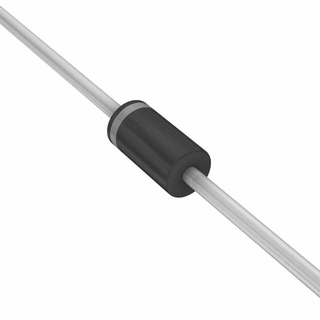
AXIAL LEAD
DO35
Note 1: Some part number series have lower JEDEC registered ratings.
Specification Features:
Zener Voltage Range = 2.4V to 200V
ESD Rating of Clas 3 (>6 KV) per Human Body Model
DO-35 Package (DO-204AH)
Double Slug Type Construction
Metallurgical Bonded Construction
Cathode
Anode
Specification Features:
Case
: Double slug type, hermetically sealed glass
Finish
: All external surfaces are corrosion resistant and leads are readily solderable
Polarity : Cathode indicated by polarity band
Mounting: Any
L
52
xx
B
Maximum Lead Temperature for Soldering Purposes
230℃, 1/16” from the case for 10 seconds
L
52xxB
= Logo
= 1N52xxB Device Code
Ordering Information
Device
Package
Quantity
1N52xxB
Axial Lead
3000 Units / Box
1N52xxBRL
Axial Lead
5000 Units / Tape & Reel
1N52xxBRL2*
Axial Lead
5000 Units / Tape & Reel
1N52xxBRR1 !
Lead Form
3000 Units / Radial Tape & Reel
1N52xxBRR2 i
Lead Form
3000 Units / Radial Tape & Reel
1N52xxBTA
Axial Lead
5000 Units / Tape & Ammo
1N52xxBTA2*
Axial Lead
5000 Units / Tape & Ammo
1N52xxBRA1 !
Axial Lead
3000 Units / Radial Tape & Ammo
1N52xxBRA2 i
Axial Lead
3000 Units / Radial Tape & Ammo
* The “2” suffix refer to 26mm tape spacing.
! “1”: Polarity band up with cathode lead off first.
i “2”: Polarity band down with cathode lead off first.
Devices listed in bold italic are Tak Cheong Preferred
devices. Preferred devices are recommended choices
for future use and best overall value.
December 2005 / B
http://takcheong.com
1
1N5221B through 1N5281B Series
®
�1N5221B through 1N5281B Series
ELECTRICAL CHARACTERISTICS (TA = 25ºC unless
otherwise noted. Based on DC measurements at thermal
equilibrium; lead length = 3/8”; thermal resistance of heat sink =
30°C/W, VF = 1.1 V Max @ IF = 200mA for all types)
Symbol
Parameter
VZ
Reverse Zener Voltage @ IZT
IZT
Reverse Zener Current
ZZT
Maximum Zener Impedance @ IZT
IZk
Reverse Zener Current
IR
Reverse Leakage Current @ VR
VR
Reverse Voltage
IF
Forward Current
VF
Forward Voltage @ IF
θVZ
Maximum Zener Voltage Temperature Coefficient
ELECTRICAL CHARACTERISTICS (TA = 25ºC unless otherwise noted, VF = 1.1 V Max @ IF = 200mA for all types)
Zener Voltage (Note 3.)
Device
(Note 2.)
Device
Marking
1N5221B
1N5222B
VZ (Volts)
Max
Zener Impedance (Note 4.)
@ IZT
ZZT @ IZT
(mA)
Ω)
(Ω
Leakage Current
θVZ
IR @ VR
(Note 5.)
ZZK @ IZK
Ω)
(Ω
(mA)
µA)
(µ
Min
Nom
(Volts)
(%/ºC)
1N5221B
2.28
2.4
2.52
20
30
1200
0.25
100
1
-0.085
1N5222B
2.375
2.5
2.625
20
30
1250
0.25
100
1
-0.085
1N5223B
1N5223B
2.565
2.7
2.835
20
30
1300
0.25
75
1
-0.08
1N5224B
1N5224B
2.66
2.8
2.94
20
30
1400
0.25
75
1
-0.08
1N5225B
1N5225B
2.85
3
3.15
20
29
1600
0.25
50
1
-0.075
1N5226B
1N5226B
3.135
3.3
3.465
20
28
1600
0.25
25
1
-0.07
1N5227B
1N5227B
3.42
3.6
3.78
20
24
1700
0.25
15
1
-0.065
1N5228B
1N5228B
3.705
3.9
4.095
20
23
1900
0.25
10
1
-0.06
1N5229B
1N5229B
4.085
4.3
4.515
20
22
2000
0.25
5
1
±0.055
1N5230B
1N5230B
4.465
4.7
4.935
20
19
1900
0.25
5
2
±0.03
1N5231B
1N5231B
4.845
5.1
5.355
20
17
1600
0.25
5
2
±0.03
1N5232B
1N5232B
5.32
5.6
5.88
20
11
1600
0.25
5
3
+0.038
1N5233B
1N5233B
5.7
6
6.3
20
7
1600
0.25
5
3.5
+0.038
1N5234B
1N5234B
5.89
6.2
6.51
20
7
1000
0.25
5
4
+0.045
1N5235B
1N5235B
6.46
6.8
7.14
20
5
750
0.25
3
5
+0.05
2. TOLERANCE AND TYPE NUMBER DESIGNATION (VZ)
The type numbers listed have a standard tolerance on the nominal zener voltage of ±5%.
3. ZENER VOLTAGE (VZ) MEASUREMENT
Nominal zener voltage is measured with the device junction in the thermal equilibrium at the lead temperature (TL) at 30°C
±1°C and 3/8” lead length.
4. ZENER IMPEDANCE (ZZ) DERIVATION
ZZT and ZZK are measured by dividing the AC voltage drop across the device by the AC current applied. The specified limits
are for IZ(AC) = 0.1 IZ(DC) with AC frequency = 60Hz.
θVZ)
5. TEMPERATURE COEFFICIENT (θ
Test conditions for temperature coefficient are as follows:
A. IZT = 7.5mA, T1 = 25°C, T2 = 125°C (1N5221B through 1N5242B)
B. IZT = Rated IZT, T1 = 25°C, T2 = 125°C (1N5243B through 1N5281B)
Device to be temperature stabilized with current applied prior to reading breakdown voltage at the specified ambient
temperature.
http://www.takcheong.com
2
�1N5221B through 1N5281B Series
ELECTRICAL CHARACTERISTICS (TA = 25ºC unless otherwise noted, VF = 1.1 V Max @ IF = 200mA for all types)
Zener Impedance (Note 8.)
Zener Voltage (Note 7.)
θVZ
IR @ VR
(Note 9.)
@ IZT
ZZT @ IZT
Max
(mA)
Ω)
(Ω
Ω)
(Ω
(mA)
µA)
(µ
(Volts)
(%/ºC)
7.875
20
6
500
0.25
3
6
+0.058
8.2
8.61
20
8
500
0.25
3
6.5
+0.062
8.7
9.135
20
8
600
0.25
3
6.5
+0.065
8.645
9.1
9.555
20
10
600
0.25
3
7
+0.068
1N5240B
9.5
10
10.5
20
17
600
0.25
3
8
+0.075
1N5241B
1N5241B
10.45
11
11.55
20
22
600
0.25
2
8.4
+0.076
1N5242B
1N5242B
11.4
12
12.6
20
30
600
0.25
1
9.1
+0.077
1N5243B
1N5243B
12.35
13
13.65
9.5
13
600
0.25
0.5
9.9
+0.079
1N5244B
1N5244B
13.3
14
14.7
9
15
600
0.25
0.1
10
+0.082
1N5245B
1N5245B
14.25
15
15.75
8.5
16
600
0.25
0.1
11
+0.082
1N5246B
1N5246B
15.2
16
16.8
7.8
17
600
0.25
0.1
12
+0.083
1N5247B
1N5247B
16.15
17
17.85
7.4
19
600
0.25
0.1
13
+0.084
1N5248B
1N5248B
17.1
18
18.9
7
21
600
0.25
0.1
14
+0.085
Device
VZ (Volts)
Leakage Current
(Note 6.)
Device
Marking
Min
Nom
1N5236B
1N5236B
7.125
7.5
1N5237B
1N5237B
7.79
1N5238B
1N5238B
8.265
1N5239B
1N5239B
1N5240B
ZZK @ IZK
1N5249B
1N5249B
18.05
19
19.95
6.6
23
600
0.25
0.1
14
+0.086
1N5250B
1N5250B
19
20
21
6.2
25
600
0.25
0.1
15
+0.086
1N5251B
1N5251B
20.9
22
23.1
5.6
29
600
0.25
0.1
17
+0.087
1N5252B
1N5252B
22.8
24
25.2
5.2
33
600
0.25
0.1
18
+0.088
1N5253B
1N5253B
23.75
25
26.25
5
35
600
0.25
0.1
19
+0.089
1N5254B
1N5254B
25.65
27
28.35
4.6
41
600
0.25
0.1
21
+0.09
1N5255B
1N5255B
26.6
28
29.4
4.5
44
600
0.25
0.1
21
+0.091
1N5256B
1N5256B
28.5
30
31.5
4.2
49
600
0.25
0.1
23
+0.091
1N5257B
1N5257B
31.35
33
34.65
3.8
58
700
0.25
0.1
25
+0.092
1N5258B
1N5258B
34.2
36
37.8
3.4
70
700
0.25
0.1
27
+0.093
1N5259B
1N5259B
37.05
39
40.95
3.2
80
800
0.25
0.1
30
+0.094
1N5260B
1N5260B
40.85
43
45.15
3
93
900
0.25
0.1
33
+0.095
1N5261B
1N5261B
44.65
47
49.35
2.7
105
1000
0.25
0.1
36
+0.095
1N5262B
1N5262B
48.45
51
53.55
2.5
125
1100
0.25
0.1
39
+0.096
1N5263B
1N5263B
53.2
56
58.8
2.2
150
1300
0.25
0.1
43
+0.096
1N5264B
1N5264B
57
60
63
2.1
170
1400
0.25
0.1
46
+0.097
1N5265B
1N5265B
58.9
62
65.1
2
185
1400
0.25
0.1
47
+0.097
6. TOLERANCE AND TYPE NUMBER DESIGNATION (VZ)
The type numbers listed have a standard tolerance on the nominal zener voltage of ±5%.
7. ZENER VOLTAGE (VZ) MEASUREMENT
Nominal zener voltage is measured with the device junction in the thermal equilibrium at the lead temperature (TL) at 30°C
±1°C and 3/8” lead length.
8. ZENER IMPEDANCE (ZZ) DERIVATION
ZZT and ZZK are measured by dividing the AC voltage drop across the device by the AC current applied. The specified limits
are for IZ(AC) = 0.1 IZ(DC) with AC frequency = 60Hz.
θVZ)
9. TEMPERATURE COEFFICIENT (θ
Test conditions for temperature coefficient are as follows:
A. IZT = 7.5mA, T1 = 25°C, T2 = 125°C (1N5221B through 1N5242B)
B. IZT = Rated IZT, T1 = 25°C, T2 = 125°C (1N5243B through 1N5281B)
Device to be temperature stabilized with current applied prior to reading breakdown voltage at the specified ambient
temperature.
http://www.takcheong.com
3
�1N5221B through 1N5281B Series
ELECTRICAL CHARACTERISTICS (TA = 25ºC unless otherwise noted, VF = 1.1 V Max @ IF = 200mA for all types)
Zener Impedance (Note 12.)
Zener Voltage (Note 11.)
IR @ VR
(Note 13.)
ZZT @ IZT
Max
(mA)
Ω)
(Ω
Ω)
(Ω
(mA)
µA)
(µ
(Volts)
(%/ºC)
68
71.4
1.8
230
1600
0.25
0.1
52
+0.097
71.25
75
78.75
1.7
270
1700
0.25
0.1
56
+0.098
77.9
82
86.1
1.5
330
2000
0.25
0.1
62
+0.098
1N5269B
82.65
87
91.35
1.4
370
2200
0.25
0.1
68
+0.099
1N5270B
1N5270B
86.45
91
95.55
1.4
400
2300
0.25
0.1
69
+0.099
1N5271B
1N5271B
95
100
105
1.3
500
2600
0.25
0.1
76
+0.11
1N5272B
1N5272B
104.5
110
115.5
1.1
750
3000
0.25
0.1
84
+0.11
1N5273B
1N5273B
114
120
126
1
900
4000
0.25
0.1
91
+0.11
1N5274B
1N5274B
123.5
130
136.5
0.95
1100
4500
0.25
0.1
99
+0.11
1N5275B
1N5275B
133
140
147
0.9
1300
4500
0.25
0.1
106
+0.11
1N5276B
1N5276B
142.5
150
157.5
0.85
1500
5000
0.25
0.1
114
+0.11
1N5277B
1N5277B
152
160
168
0.8
1700
5500
0.25
0.1
122
+0.11
1N5278B
1N5278B
161.5
170
178.5
0.74
1900
5500
0.25
0.1
129
+0.11
1N5279B
1N5279B
171
180
189
0.68
2200
6000
0.25
0.1
137
+0.11
1N5280B
1N5280B
180.5
190
199.5
0.66
2400
6500
0.25
0.1
144
+0.11
1N5281B
1N5281B
190
200
210
0.65
2500
7000
0.25
0.1
152
+0.11
(Note 10.)
Device
Marking
Min
Nom
1N5266B
1N5266B
64.6
1N5267B
1N5267B
1N5268B
1N5268B
1N5269B
ZZK @ IZK
θVZ
@ IZT
Device
VZ (Volts)
Leakage Current
10. TOLERANCE AND TYPE NUMBER DESIGNATION (VZ)
The type numbers listed have a standard tolerance on the nominal zener voltage of ±5%.
11. ZENER VOLTAGE (VZ) MEASUREMENT
Nominal zener voltage is measured with the device junction in the thermal equilibrium at the lead temperature (TL) at 30°C
±1°C and 3/8” lead length.
12. ZENER IMPEDANCE (ZZ) DERIVATION
ZZT and ZZK are measured by dividing the AC voltage drop across the device by the AC current applied. The specified limits
are for IZ(AC) = 0.1 IZ(DC) with AC frequency = 60Hz.
θVZ)
13. TEMPERATURE COEFFICIENT (θ
Test conditions for temperature coefficient are as follows:
A. IZT = 7.5mA, T1 = 25°C, T2 = 125°C (1N5221B through 1N5242B)
B. IZT = Rated IZT, T1 = 25°C, T2 = 125°C (1N5243B through 1N5281B)
Device to be temperature stabilized with current applied prior to reading breakdown voltage at the specified ambient
temperature.
http://www.takcheong.com
4
�1N5221B through 1N5281B Series
0.7
HEAT
SINKS
P D , MAXIMUM STEADY STATE
POWER DISSIPATION (WATTS)
0.6
0.5
0.4
3/8"
3/8"
0.3
0.2
0.1
0
0
20
40
60
80
100
120
140
160
T L , LEAD TEMPERATURE (°C)
Figure 1. Steady State Power Derating
http://www.takcheong.com
5
180
200
�1N5221B through 1N5281B Series
Since the actual voltage available from a given zener
diode is temperature dependent, it is necessary to determine
junction temperature under any set of operating conditions
in order to calculate its value. The following procedure is
recommended:
Lead Temperature, TL, should be determined from:
TL = θLAPD + TA.
θLA is the lead-to-ambient thermal resistance (°C/W) and PD
is the power dissipation. The value for θLA will vary and
depends on the device mounting method. θLA is generally 30
to 40°C/W for the various clips and tie points in common use
and for printed circuit board wiring.
The temperature of the lead can also be measured using a
thermocouple placed on the lead as close as possible to the
tie point. The thermal mass connected to the tie point is
normally large enough so that it will not significantly
respond to heat surges generated in the diode as a result of
pulsed operation once steady-state conditions are achieved.
Using the measured value of TL, the junction temperature
may be determined by:
θJL, JUNCTION TO LEAD THERMAL RESISTANCE ( ° C/W)
APPLICATION NOTE - ZENER VOLTAGE
L
2.4-60 V
200
62-200 V
100
0
0
0.2
0.4
1000
7000
5000
0.6
0.8
1
TYPICAL LEAKAGE CURRENT
AT 80% OF NOMINAL
BREAKDOWN VOLTAGE
2000
1000
700
500
200
∆TJL = θJLPD.
100
70
50
I R , LEAKAGE CURRENT ( µ A)
θVZ, the zener voltage temperature coefficient, is found
from Figures 4 and 5.
Under high power-pulse operation, the zener voltage will
vary with time and may also be affected significantly by the
zener resistance. For best regulation, keep current
excursions as low as possible.
Surge limitations are given in Figure 7. They are lower
than would be expected by considering only junction
temperature, as current crowding effects cause temperatures
to be extremely high in small spots, resulting in device
degradation should the limits of Figure 7 be exceeded.
L
300
Figure 2. Typical Thermal Resistance
∆TJL is the increase in junction temperature above the lead
temperature and may be found from Figure 2 for dc power:
∆V = θVZTJ.
400
L , LEAD LENGTH TO HEAT SINK (INCH)
TJ = TL + ∆TJL.
For worst-case design, using expected limits of IZ, limits
of PD and the extremes of TJ(∆TJ) may be estimated.
Changes in voltage, VZ, can then be found from:
500
20
10
7
5
2
1
0.7
0.5
+125°C
0.2
0.1
0.07
0.05
0.02
0.01
0.007
0.005
+25°C
0.002
0.001
3
4
5
6
7
8
9
10
11
12
VZ , NOMINAL ZENER VOLTAGE (VOLTS)
Figure 3. Typical Leakage Current
http://www.takcheong.com
6
13
14
15
�1N5221B through 1N5281B Series
TEMPERATURE COEFFICIENTS
TEMPERATURE COEFFICIENT (mV/ °C)
+12
+10
+8
+6
+4
+2
RANGE
VZ @ IZT
(NOTE 2)
0
-2
θ VZ ,
θ VZ ,
TEMPERA TURE COEFFICIENT (mV/ °C)
(-55 °C to +150 °C temperature range; 90% of the units are in the ranges indicated.)
-4
2
4
3
5
6
7
8
10
9
11
100
70
50
30
20
5
3
2
1
10
12
20
TEMPERATURE COEFFICIENT (mV/°C)
160
140
VZ @ IZT
(NOTE 2)
θ VZ ,
TEMPERA TURE COEFFICIENT (mV/°C)
θ VZ ,
180
100
140
150
160
170
70
100
180
190
+6
VZ @ IZ
TA= 25 °C
+4
+2
20mA
0
0.01mA
1mA
-2
NOTE: BELOW 3 VOLTS AND ABOVE 8 VOL TS
NOTE: CHANGES IN ZENER CURRENT DO NOT
NOTE: AFFECT TEMPERATURE COEFFICIENTS
-4
3
200
6
5
4
8
7
V Z , ZENER VOLTAGE (VOLTS)
V Z , ZENER VOLTAGE (VOLTS)
Figure 4c. Range for Units 120 to 200 Volts
Figure 5. Effect of Zener Current
1000
100
TA = 25 ° C
70
500
T= 25 °C
50
0V BIAS
0 BIAS
C, CAP ACIT ANCE (pF)
200
C, CAP ACIT ANCE (pF)
50
Figure 4b. Range for Units 12 to 100 Volts
200
130
30
V Z , ZENER VOLTAGE (VOLTS)
Figure 4a. Range for Units to 12 Volts
120
(NOTE 2)
7
V Z , ZENER VOLTAGE (VOLTS)
120
VZ @ IZ
RANGE
10
100
1V BIAS
50
20
10
50% OF
V Z BIAS
5
30
20
1 VOLT BIAS
10
7
50% OF V BIAS
5
3
2
2
1
1
1
2
5
10
20
50
100
120
140
Figure 6a. Typical Capacitance 2.4-100 Volts
160
180
190
200
V Z, ZENER VOLTAGE (VOLTS)
V Z, ZENER VOLTAGE (VOLTS)
Figure 6b. Typical Capacitance 120-200 Volts
http://www.takcheong.com
7
220
�1N5221B through 1N5281B Series
Ppk , PEAK SURGE POWER (WATTS)
100
70
50
RECT ANGULAR
WAVEFORM
T J = 25°C PRIOR TO
INITIAL PULSE
11V-91V NONREPETITIVE
30
5% DUTY CYCLE
1.8V-10V NONREPETITIVE
20
10
10% DUTY CYCLE
7
5
20% DUTY CYCLE
3
2
1
0.01
0.02
0.05
0.1
0.2
0.5
1
2
5
10
20
50
100
200
500
1000
PW, PULSE WIDTH (ms)
Figure 7a. Maximum Surge Power 1.8-91 Volts
1000
RECT ANGULAR
WAVEFORM, TJ = 25 °C
300
200
100
70
50
100-200 VOLTS NONREPETITIVE
30
20
10
7
5
3
2
1
0.01
T J = 25°C
iZ (rms) = 0.1 Iz(dc)
VZ = 2.7V
f = 60 Hz
200
47V
100
27V
50
20
6.2V
10
5
2
1
0.1
1
10
100
0.1
1000
0.2
0.5
1
2
5
10
20
PW, PULSE WIDTH (ms)
IZ , ZENER CURRENT (mA)
Figure 7b. Maximum Surge Power DO-35
100-200Volts
Figure 8. Effect of Zener Current on
Zener Impedance
1000
700
500
Z Z , DYNAMIC IMPEDANCE (OHMS)
Z Z , DYNAMIC IMPEDANCE (OHMS)
500
TJ = 25°C
200
100
70
50
5mA
20
20mA
100
MAXIMUM
500
f = 60Hz
IZ = 1mA
50
1000
iZ (rms) = 0.1 IZ (dc)
I F , FOR WARD CURRENT (mA)
Ppk , PEAK SURGE POWER (WATTS)
1000
700
500
10
7
5
2
MINIMUM
200
100
50
75 °C
20
10
25 °C
5 150 °C
0 °C
2
1
1
1
2
3
5
7
10
20
30
50
70 100
0.4
0.5
V Z , ZENER VOLTAGE (VOLTS)
0.6
0.7
0.8
0.9
1
V F , FORWARD VOLTAGE (VOLTS)
Figure 9. Effect of Zener Voltage on Zener Impedance
Figure 10. Typical Forward Characteristics
http://www.takcheong.com
8
1.1
�1N5221B through 1N5281B Series
20
10
I Z , ZENER CURRENT
(mA)
TA = 25°C
1
0.1
0.01
1
2
3
4
5
6
7
8
9
10
11
12
13
14
15
16
29
30
V Z , ZENER VOLTAGE (VOLTS)
Figure 1 1. Zener Voltage versus Zener Current - VZ = 1 thru 16 Volts
10
I Z , ZENER CURRENT
(mA)
TA = 25°C
1
0.1
0.01
15
16
17
18
19
20
21
22
23
24
25
26
27
V Z , ZENER VOLTAGE (VOLTS)
Figure 12. Zener Voltage versus Zener Current - VZ = 15 thru 30 Volts
http://www.takcheong.com
9
28
�1N5221B through 1N5281B Series
I Z , ZENER CURRENT
(mA)
10
TA = 25°
1
0.1
0.01
30
35
40
45
50
55
65
60
70
75
80
85
95
100
105
240
250
260
90
V Z , ZENER VOLTAGE (VOLTS)
Figure 13. Zener Voltage versus Zener Current - VZ = 30 thru 105 Volts
I Z , ZENER CURRENT
(mA)
10
1
0.1
0.01
110
120
130
140
150
160
170
180
190
200
210
220
230
V Z , ZENER VOLTAGE (VOLTS)
Figure 14. Zener Voltage versus Zener Current - VZ = 110 thru 220 Volts
http://www.takcheong.com
10
�


 工商网监
湘ICP备2023018690号
工商网监
湘ICP备2023018690号
