2N5088 / MMBT5088 / 2N5089 / MMBT5089
2N5088 2N5089
MMBT5088 MMBT5089
C
E C B
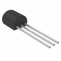
TO-92
E
SOT-23
Mark: 1Q / 1R
B
NPN General Purpose Amplifier
This device is designed for low noise, high gain, general purpose amplifier applications at collector currents from 1µA to 50 mA.
Absolute Maximum Ratings*
Symbol
VCEO VCBO VEBO IC TJ, Tstg Collector-Emitter Voltage Collector-Base Voltage Emitter-Base Voltage Collector Current - Continuous
TA = 25°C unless otherwise noted
Parameter
2N5088 2N5089 2N5088 2N5089
Value
30 25 35 30 4.5 100 -55 to +150
Units
V V V V V mA °C
Operating and Storage Junction Temperature Range
*These ratings are limiting values above which the serviceability of any semiconductor device may be impaired.
NOTES: 1) These ratings are based on a maximum junction temperature of 150 degrees C. 2) These are steady state limits. The factory should be consulted on applications involving pulsed or low duty cycle operations.
Thermal Characteristics
Symbol
TA = 25°C unless otherwise noted
Characteristic
2N5088 2N5089 625 5.0 83.3 200
Max
*MMBT5088 *MMBT5089 350 2.8 357
Units
PD RθJC R θJ A
Total Device Dissipation Derate above 25°C Thermal Resistance, Junction to Case Thermal Resistance, Junction to Ambient
mW mW/°C °C/W °C/W
*Device mounted on FR-4 PCB 1.6" X 1.6" X 0.06."
2 001 Fairchild Semiconductor C orporation
2N5088/2N5089/MMBT5088/MMBT5089, Rev A
�2N5088 / MMBT5088 / 2N5089 / MMBT5089
NPN General Purpose Amplifier
(continued)
Electrical Characteristics
Symbol Parameter
TA = 25°C unless otherwise noted
Test Conditions
Min
Max
Units
OFF CHARACTERISTICS
V(BR)CEO V(BR)CBO ICBO IEBO Collector-Emitter Breakdown Voltage* Collector-Base Breakdown Voltage Collector Cutoff Current Emitter Cutoff Current IC = 1.0 mA, IB = 0 IC = 100 µA, IE = 0 VCB = 20 V, IE = 0 VCB = 15 V, IE = 0 VEB = 3.0 V, IC = 0 VEB = 4.5 V, IC = 0 5088 5089 5088 5089 5088 5089 30 25 35 30 50 50 50 100 V V V V nA nA nA nA
ON CHARACTERISTICS
hFE DC Current Gain IC = 100 µA, VCE = 5.0 V IC = 1.0 mA, VCE = 5.0 V IC = 10 mA, VCE = 5.0 V* VCE(sat) VBE(on) Collector-Emitter Saturation Voltage Base-Emitter On Voltage IC = 10 mA, IB = 1.0 mA IC = 10 mA, VCE = 5.0 V 5088 5089 5088 5089 5088 5089 300 400 350 450 300 400 900 1200
0.5 0.8
V V
SMALL SIGNAL CHARACTERISTICS
fT Ccb Ceb hfe NF Current Gain - Bandwidth Product Collector-Base Capacitance Emitter-Base Capacitance Small-Signal Current Gain Noise Figure IC = 500 µA,VCE = 5.0 mA, f = 20 MHz VCB = 5.0 V, IE = 0, f = 100 kHz VBE = 0.5 V, IC = 0, f = 100 kHz IC = 1.0 mA, VCE = 5.0 V, f = 1.0 kHz IC = 100 µA, VCE = 5.0 V, RS = 1 0 k Ω , f = 10 Hz to 15.7 kHz 5088 5089 5088 5089 350 450 50 4.0 10 1400 1800 3.0 2.0 MHz pF pF
3
dB dB
*Pulse Test: Pulse Width ≤ 300 µs, Duty Cycle ≤ 2.0%
Spice Model
NPN (Is=5.911f Xti=3 Eg=1.11 Vaf=62.37 Bf=1.122K Ne=1.394 Ise=5.911f Ikf=14.92m Xtb=1.5 Br=1.271 Nc=2 Isc=0 Ikr=0 Rc=1.61 Cjc=4.017p Mjc=.3174 Vjc=.75 Fc=.5 Cje=4.973p Mje=.4146 Vje=.75 Tr=4.673n Tf=821.7p Itf=.35 Vtf=4 Xtf=7 Rb=10)
�2N5088 / MMBT5088 / 2N5089 / MMBT5089
NPN General Purpose Amplifier
(continued)
Typical Characteristics
1200 1000 800 600
25 °C 125 °C
VCESAT - COLLECTOR-EMITTER VOLTAGE (V)
h FE - TYPICAL PULSED CURRENT GAIN
Typical Pulsed Current Gain vs Collector Current
V CE = 5.0 V
Collector-Emitter Saturation Voltage vs Collector Current
0.3 0.25 0.2
125 °C
β = 10
0.15 0.1 0.05 0.1
25 °C - 40 °C
400
- 40 °C
200 0 0.01 0.03 0.1 0.3 1 3 10 30 I C - COLLECTOR CURRENT (mA) 100
1 10 I C - COLLECTOR CURRENT (mA)
100
VBESAT - COLLECTOR-EMITTER VOLTAGE (V)
1
- 40 ° C
VBEON- BASE-EMITTER ON VOLTAGE (V)
Base-Emitter Saturation Voltage vs Collector Current
Base-Emitter ON Voltage vs Collector Current
1 0.8 0.6
125 ° C - 40 ° C 25 ° C
0.8 0.6 0.4 0.2 0.1 1 10 I C - COLLECTOR CURRENT (mA) 100
25 ° C 125 ° C
β = 10
0.4
V CE = 5.0 V
0.2 0.1 1 10 I C - COLLECTOR CURRENT (mA) 40
Collector-Cutoff Current vs Ambient Temperature
I CBO - COLLE CTOR CURRENT (nA) 10 VCB = 45V
1
0.1 25
50 75 100 125 T A - AMBIE NT TEMP ERATURE ( ° C)
150
�2N5088 / MMBT5088 / 2N5089 / MMBT5089
NPN General Purpose Amplifier
(continued)
Typical Characteristics
(continued)
Input and Output Capacitance vs Reverse Bias Voltage
f = 1.0 MHz CAPACITANCE (pF) 4 3
C te
Contours of Constant Gain Bandwidth Product (f T )
V CE - COLLECTOR VOLTAGE (V) 10 7 5
150 MHz 175 MHz
5
3 2
2 1 0
C ob
125 MHz 100 MHz 75 MHz
0
4
8 12 16 REVERSE BIAS VOLTAGE (V)
20
1 0.1
1 10 I C - COLLECTOR CURRENT (mA)
100
CHARACTERIS TIC S RELATI VE TO VALUE AT T A = 25 C
Normalized Collector-Cutoff Current vs Ambient Temperature
5 NF - NOISE FIGURE (dB)
Wideband Noise Frequency vs Source Resistance
V CE = 5.0 V
°
1000
4 3 2 1 0
BANDWIDTH = 15.7 kHz
100
I C = 100 µA I C = 30 µA
3
10
I C = 10 µA
2,000 5,000 10,000 20,000 50,000 100,000
1 25
50 75 100 125 T A - AMBIE NT TEMPERATURE ( °C)
150
1,000
R S - SOURCE RESISTANCE (Ω )
Noise Figure vs Frequency
10
P D - POWER DISSIPATION (mW)
Power Dissipation vs Ambient Temperature
625
NF - NOISE FIGURE (dB)
8
I C = 200 µA, R S = 10 kΩ I C = 100 µA, R S = 10 kΩ I C = 1.0 mA, R S = 500 Ω
TO-92
500 375 250 125 0
6
SOT-23
4
I C = 1.0 mA, R S = 5.0 kΩ V CE = 5.0V
2
0 0.0001
0.001
0.01 0.1 1 f - FREQUENCY (MHz)
10
100
0
25
50 75 100 TEMPERATURE ( o C)
125
150
�2N5088 / MMBT5088 / 2N5089 / MMBT5089
NPN General Purpose Amplifier
(continued)
Typical Characteristics
(continued)
Contours of Constant Narrow Band Noise Figure
R S - SOURCE RESISTANCE ( Ω )
3.0 dB
5,000
Contours of Constant Narrow Band Noise Figure
R S - SOURCE RESISTANCE ( Ω )
10,000 5,000
10,000
4.0 dB
2,000 1,000 500
V CE = 5.0 V
2.0 dB
2,000
6.0 dB 8.0 dB 10 dB
f = 100 Hz BANDWIDTH = 20 Hz
3.0 dB
1,000
4.0 dB
500
V CE = 5.0 V f = 1.0 kHz BANDWIDTH = 200 Hz
6.0 dB 8.0 dB
200 100
12 dB 14 dB
200 100
1
10 100 I C - COLLECTOR CURRENT ( µ A)
1,000
1
10 100 I C- COLLECTOR CURRENT ( µ A)
1,000
Contours of Constant Narrow Band Noise Figure
R S - SOURCE RESISTANCE (Ω ) 5000 2000 1000 500 200 100 1 V CE = 5.0V f = 10kHz BANDWIDTH = 2.0kHz R S - SOURCE RESISTANCE (Ω ) 10000
1.0 dB 2.0 dB 3.0 dB 4.0 dB 6.0 dB 8.0 dB
Contours of Constant Narrow Band Noise Figure
10000 5000 2000 1000 500
2.0 dB
3.0 dB 5.0 dB 6.0 dB
10 100 I C - COLLECTOR CURRENT ( µ A)
1000
VCE = 4.0 dB 5.0V f = 1.0 MHz 200 BANDWIDTH 7.0 dB = 200kHz 8.0 dB 100 0.01 0.1 1 I C - COLLECTOR CURRENT ( µ A)
10
�2N5088 / MMBT5088 / 2N5089 / MMBT5089
NPN General Purpose Amplifier
(continued)
Typical Common Emitter Characteristics
(f = 1.0 kHz)
C HAR ACTER ISTI CS RELATI VE TO VALUE(VCE =5V)
1.4
h fe
C HARACTE RI STICS RE LATIV E TO VA LUE (TA =25° C)
Typical Common Emitter Characteristics
1.3
h ie
Typical Common Emitter Characteristics
1.5 1.4 1.3 1.2 1.1 1 0.9 0.8 0.7 0.6 0.5 -100
h oe h fe h re h ie
1.2 1.1
h re
h oe h re h oe
VCE = 5 .0V f = 1.0kHz I C = 1.0mA
h ie
h re h fe h oe
1 h ie 0.9 0.8 I C = 1 .0mA f = 1.0kHz T A = 25°C 5 10 15 20 V CE - COLLECTOR VOLTAGE (V) 25
h fe
0
-50 0 50 100 T J - JUNCTIO N TEMP ERATURE (° C)
150
Typical Common Emitter Characteristics
CHARACTERISTICS RELATIVE TO VALUE(I C =1mA)
100 f = 1.0kHz 10
h ie a nd h re h re h oe
1 h oe
h fe
3
0.1
h ie
h fe
0.01 0.1
0.2
0.5 1 2 5 10 20 I C - COLLECTOR CURRENT (mA)
50
100
�TRADEMARKS
The following are registered and unregistered trademarks Fairchild Semiconductor owns or is authorized to use and is not intended to be an exhaustive list of all such trademarks.
ACEx™ Bottomless™ CoolFET™ CROSSVOLT™ DOME™ E2CMOSTM EnSignaTM FACT™ FACT Quiet Series™ FAST
DISCLAIMER
FASTr™ GlobalOptoisolator™ GTO™ HiSeC™ ISOPLANAR™ MICROWIRE™ OPTOLOGIC™ OPTOPLANAR™ PACMAN™ POP™
PowerTrench QFET™ QS™ QT Optoelectronics™ Quiet Series™ SILENT SWITCHER SMART START™ SuperSOT™-3 SuperSOT™-6 SuperSOT™-8
SyncFET™ TinyLogic™ UHC™ VCX™
FAIRCHILD SEMICONDUCTOR RESERVES THE RIGHT TO MAKE CHANGES WITHOUT FURTHER NOTICE TO ANY PRODUCTS HEREIN TO IMPROVE RELIABILITY, FUNCTION OR DESIGN. FAIRCHILD DOES NOT ASSUME ANY LIABILITY ARISING OUT OF THE APPLICATION OR USE OF ANY PRODUCT OR CIRCUIT DESCRIBED HEREIN; NEITHER DOES IT CONVEY ANY LICENSE UNDER ITS PATENT RIGHTS, NOR THE RIGHTS OF OTHERS.
LIFE SUPPORT POLICY FAIRCHILD’S PRODUCTS ARE NOT AUTHORIZED FOR USE AS CRITICAL COMPONENTS IN LIFE SUPPORT DEVICES OR SYSTEMS WITHOUT THE EXPRESS WRITTEN APPROVAL OF FAIRCHILD SEMICONDUCTOR CORPORATION. As used herein: 1. Life support devices or systems are devices or 2. A critical component is any component of a life support device or system whose failure to perform can systems which, (a) are intended for surgical implant into be reasonably expected to cause the failure of the life the body, or (b) support or sustain life, or (c) whose support device or system, or to affect its safety or failure to perform when properly used in accordance with instructions for use provided in the labeling, can be effectiveness. reasonably expected to result in significant injury to the user. PRODUCT STATUS DEFINITIONS Definition of Terms Datasheet Identification Advance Information Product Status Formative or In Design Definition This datasheet contains the design specifications for product development. Specifications may change in any manner without notice. This datasheet contains preliminary data, and supplementary data will be published at a later date. Fairchild Semiconductor reserves the right to make changes at any time without notice in order to improve design. This datasheet contains final specifications. Fairchild Semiconductor reserves the right to make changes at any time without notice in order to improve design.
Preliminary
First Production
No Identification Needed
Full Production
Obsolete
Not In Production
This datasheet contains specifications on a product that has been discontinued by Fairchild semiconductor. The datasheet is printed for reference information only.
Rev. G
�