74ACT153MTC

74ACT153MTC

  • 厂商:

    FAIRCHILD(仙童半导体)

  • 封装:

  • 描述:

    74ACT153MTC - Dual 4-Input Multiplexer - Fairchild Semiconductor

  • 详情介绍
  • 数据手册
  • 价格&库存
74ACT153MTC 数据手册
74AC153 • 74ACT153 Dual 4-Input Multiplexer November 1988 Revised November 1999 74AC153 • 74ACT153 Dual 4-Input Multiplexer General Description The AC/ACT153 is a high-speed dual 4-input multiplexer with common select inputs and individual enable inputs for each section. It can select two lines of data from four sources. The two buffered outputs present data in the true (non-inverted) form. In addition to multiplexer operation, the AC/ACT153 can act as a function generator and generate any two functions of three variables. Features s ICC reduced by 50% s Outputs source/sink 24 mA s ACT153 has TTL-compatible inputs Ordering Code: Order Number 74AC153SC 74AC153SJ 74AC153MTC 74AC153PC 74ACT153SC 74ACT153MTC Package Number M16A M16D MTC16 N16E M16A MTC16 Package Description 16-Lead Small Outline Integrated Circuit (SOIC), JEDEC MS-012, 0.150” Narrow Body 16-Lead Small Outline Package (SOP), EIAJ TYPE II, 5.3mm Wide 16-Lead Thin Shrink Small Outline Package (TSSOP), JEDEC MO-153, 4.4mm Wide 16-Lead Plastic Dual-In-Line Package (PDIP), JEDEC MS-001, 0.300” Wide 16-Lead Small Outline Integrated Circuit (SOIC), JEDEC MS-012, 0.150” Narrow Body 16-Lead Thin Shrink Small Outline Package (TSSOP), JEDEC MO-153, 4.4mm Wide Device also available in Tape and Reel. Specify by appending suffix letter “X” to the ordering code. Logic Symbols Connection Diagram IEEE/IEC Pin Descriptions Pin Names I0a–I3a I0b–I3b S0 , S1 Ea Eb Za Zb Description Side A Data Inputs Side B Data Inputs Common Select Inputs Side A Enable Input Side B Enable Input Side A Output Side B Output FACT is a trademark of Fairchild Semiconductor Corporation. © 1999 Fairchild Semiconductor Corporation DS009928 www.fairchildsemi.com 74AC153 • 74ACT153 Functional Description The AC/ACT153 is a dual 4-input multiplexer. It can select two bits of data from up to four sources under the control of the common Select inputs (S0, S1). The two 4-input multiplexer circuits have individual active-LOW Enables (Ea, Eb) which can be used to strobe the outputs independently. When the Enables (Ea, Eb) are HIGH, the corresponding outputs Za, Zb) are forced LOW. The AC/ACT153 is the logic implementation of a 2-pole, 4-position switch, where the position of the switch is determined by the logic levels supplied to the Select inputs. The logic equations for the outputs are shown below. Za = Ea • (I0a • S1 • S0 + I1a • S1 • S0 + I2a • S1 • S0 + I3a • S1 • S0) Zb = Eb • (I0b • S1 • S0 + I1b • S1 • S0 + I2b • S1 • S0 + I3b • S1 • S0) Truth Table Select Inputs S0 X L L H H L L H H S1 X L L L L H H H H E H L L L L L L L L Inputs (a or b) I0 X L H X X X X X X I1 X X X L H X X X X I2 X X X X X L H X X I3 X X X X X X X L H Output Z L L H L H L H L H H = H IGH Voltage Level L = LOW Voltage Level X = Immaterial Logic Diagram Please note that this diagram is provided only for the understanding of logic operations and should not be used to estimate propagation delays. www.fairchildsemi.com 2 74AC153 • 74ACT153 Absolute Maximum Ratings(Note 1) Supply Voltage (VCC) DC Input Diode Current (IIK) VI = −0.5V VI = VCC + 0.5V DC Input Voltage (VI) DC Output Diode Current (IOK) VO = −0.5V VO = VCC + 0.5V DC Output Voltage (VO) DC Output Source or Sink Current (IO) DC VCC or Ground Current per Output Pin (ICC or IGND) Storage Temperature (TSTG) Junction Temperature (TJ) PDIP 140°C ±50 mA −65°C to +150 °C ±50 mA −20 mA +20 mA −0.5V to VCC + 0.5V −20 mA +20 mA −0.5V to VCC + 0.5V −0.5V to +7.0V Recommended Operating Conditions Supply Voltage (VCC) AC ACT Input Voltage (VI) Output Voltage (VO) Operating Temperature (TA) Minimum Input Edge Rate (∆V/∆t) AC Devices VIN from 30% to 70% of VCC VCC @ 3.3V, 4.5V, 5.5V Minimum Input Edge Rate (∆V/∆t) ACT Devices VIN from 0.8V to 2.0V VCC @ 4.5V, 5.5V 125 mV/ns Note 1: Absolute maximum ratings are those values beyond which damage to the device may occur. The databook specifications should be met, without exception, to ensure that the system design is reliable over its power supply, temperature, and output/input loading variables. Fairchild does not recommend operation of FACT circuits outside databook specifications. 2.0V to 6.0V 4.5V to 5.5V 0V to VCC 0V to VCC −40°C to +85°C 125 mV/ns DC Electrical Characteristics for AC Symbol VIH Parameter Minimum HIGH Level Input Voltage VIL Maximum LOW Level Input Voltage VOH Minimum HIGH Level Output Voltage VCC (V) 3.0 4.5 5.5 3.0 4.5 5.5 3.0 4.5 5.5 3.0 4.5 5.5 VOL Maximum LOW Level Output Voltage 3.0 4.5 5.5 3.0 4.5 5.5 IIN (Note 4) IOLD IOHD ICC (Note 4) Maximum Input Leakage Current Minimum Dynamic Output Current (Note 3) Maximum Quiescent Supply Current 5.5 5.5 5.5 5.5 4.0 0.002 0.001 0.001 TA = +25°C Typ 1.5 2.25 2.75 1.5 2.25 2.75 2.99 4.49 5.49 2.1 3.15 3.85 0.9 1.35 1.65 2.9 4.4 5.4 2.56 3.86 4.86 0.1 0.1 0.1 0.36 0.36 0.36 ±0.1 TA = −40°C to +85°C Guaranteed Limits 2.1 3.15 3.85 0.9 1.35 1.65 2.9 4.4 5.4 VIN = VIL or VIH 2.46 3.76 4.76 0.1 0.1 0.1 VIN = VIL or VIH 0.44 0.44 0.44 ±1.0 75 −75 40.0 µA mA mA µA V IOL = 12 mA IOL = 24 mA IOL = 24 mA (Note 2) VI = VCC, GND VOLD = 1.65V Max VOHD = 3.85V Min VIN = VCC or GND V IOUT = 50 µA V IOH = −12 mA IOH = −24 mA IOH = −24 mA (Note 2) V IOUT = −50 µA V VOUT = 0.1V or VCC − 0.1V V Units Conditions VOUT = 0.1V or VCC − 0.1V Note 2: All outputs loaded; thresholds on input associated with output under test. Note 3: M aximum test duration 2.0 ms, one output loaded at a time. Note 4: IIN and ICC @ 3.0V are guaranteed to be less than or equal to the respective limit @ 5.5V VCC. 3 www.fairchildsemi.com 74AC153 • 74ACT153 DC Electrical Characteristics for ACT Symbol VIH VIL VOH Parameter Minimum HIGH Level Input Voltage Maximum LOW Level Input Voltage Minimum HIGH Level Output Voltage VCC (V) 4.5 5.5 4.5 5.5 4.5 5.5 4.5 5.5 VOL Maximum LOW Level Output Voltage 4.5 5.5 4.5 5.5 IIN ICCT IOLD IOHD ICC Maximum Input Leakage Current Maximum ICC/Input Minimum Dynamic Output Current (Note 6) Maximum Quiescent Supply Current 5.5 5.5 5.5 5.5 5.5 4.0 0.6 0.001 0.001 TA = +25°C Typ 1.5 1.5 1.5 1.5 4.49 5.49 2.0 2.0 0.8 0.8 4.4 5.4 3.86 4.86 0.1 0.1 0.36 0.36 ±0.1 TA = −40°C to +85°C Guaranteed Limits 2.0 2.0 0.8 0.8 4.4 5.4 3.76 4.76 0.1 0.1 0.44 0.44 ±1.0 1.5 75 −75 40.0 µA mA mA mA µA V Units V V V Conditions VOUT = 0.1V or VCC − 0.1V VOUT = 0.1V or VCC − 0.1V IOUT = −50 µA VIN = VIL or VIH V IOH = − 24 mA IOH = − 24 mA (Note 5) IOUT = 50 µA VIN = VIL or VIH V IOL = 24 mA IOL = 24 mA (Note 5) VI = V CC, GND VI = V CC − 2.1V VOLD = 1.65V Max VOHD = 3.85V Min VIN = VCC or GND Note 5: All outputs loaded; thresholds on input associated with output under test. Note 6: Maximum test duration 2.0 ms, one output loaded at a time. AC Electrical Characteristics for AC VCC Symbol Parameter (V) (Note 7) tPLH tPHL tPLH Propagation Delay Sn to Zn Propagation Delay Sn to Zn Propagation Delay E to Zn tPHL Propagation Delay E to Zn tPLH tPHL Propagation Delay In to Zn Propagation Delay In to Zn Note 7: Voltage Range 3.3 is 3.3V ± 0 3V Voltage Range 5.0 is 5.0V ± 0.5V TA = +25°C CL = 50 pF Min 2.5 2.0 3.0 2.5 2.5 1.5 2.5 2.0 2.5 1.5 1.5 1.5 Typ 9.5 6.5 8.5 6.5 8.0 5.5 7.0 5.0 7.5 5.5 7.0 5.0 Max 15.0 11.0 14.5 11.0 13.5 9.5 11.0 8.0 12.5 9.0 11.5 8.5 TA = −40°C to +85°C CL = 50 pF Min 2.5 2.0 2.5 2.0 2.0 1.5 2.0 1.5 2.0 1.5 1.5 1.5 Max 17.5 12.5 16.5 12.0 16.0 11.0 12.5 9.0 14.5 10.5 13.0 10.0 ns ns ns ns Units 3.3 5.0 3.3 5.0 3.3 5.0 3.3 5.0 3.3 5.0 3.3 5.0 ns ns www.fairchildsemi.com 4 74AC153 • 74ACT153 AC Electrical Characteristics for ACT VCC Symbol tPLH tPHL tPLH Parameter Propagation Delay S n to Z n Propagation Delay S n to Z n Propagation Delay 5.0 E n to Z n tPHL Propagation Delay 5.0 E n to Z n tPLH tPHL Propagation Delay In to Zn Propagation Delay In to Zn Note 8: Voltage Range 5.0 is 5.0V ± 0.5V TA = +25°C CL = 50 pF Min 3.0 3.0 Typ 7.0 7.0 Max 11.5 11.5 TA = −40°C to +85°C CL = 50 pF Min 2.0 2.5 Max 13.5 13.5 ns ns Units (V) (Note 8) 5.0 5.0 2.0 6.5 10.5 2.0 12.5 ns 3.0 6.0 9.5 2.5 11.0 ns 5.0 5.0 2.5 2.0 5.5 5.5 9.5 9.5 2.0 2.0 11.0 11.0 ns ns Capacitance Symbol CIN CPD Parameter Input Capacitance Power Dissipation Capacitance Typ 4.5 65.0 Units pF pF VCC = OPEN VCC = 5.0V Conditions 5 www.fairchildsemi.com 74AC153 • 74ACT153 Physical Dimensions inches (millimeters) unless otherwise noted 16-Lead Small Outline Integrated Circuit (SOIC), JEDEC MS-012, 0.150” Narrow Body Package Number M16A www.fairchildsemi.com 6 74AC153 • 74ACT153 Physical Dimensions inches (millimeters) unless otherwise noted (Continued) 16-Lead Small Outline Package (SOP), EIAJ TYPE II, 5.3mm Wide Package Number M16D 7 www.fairchildsemi.com 74AC153 • 74ACT153 Physical Dimensions inches (millimeters) unless otherwise noted (Continued) 16-Lead Thin Shrink Small Outline Package (TSSOP), JEDEC MO-153, 4.4mm Wide Package Number MTC16 www.fairchildsemi.com 8 74AC153 • 74ACT153 Dual 4-Input Multiplexer Physical Dimensions inches (millimeters) unless otherwise noted (Continued) 16-Lead Plastic Dual-In-Line Package (PDIP), JEDEC MS-001, 0.300” Wide Package Number N16E Fairchild does not assume any responsibility for use of any circuitry described, no circuit patent licenses are implied and Fairchild reserves the right at any time without notice to change said circuitry and specifications. LIFE SUPPORT POLICY FAIRCHILD’S PRODUCTS ARE NOT AUTHORIZED FOR USE AS CRITICAL COMPONENTS IN LIFE SUPPORT DEVICES OR SYSTEMS WITHOUT THE EXPRESS WRITTEN APPROVAL OF THE PRESIDENT OF FAIRCHILD SEMICONDUCTOR CORPORATION. As used herein: 1. Life support devices or systems are devices or systems which, (a) are intended for surgical implant into the body, or (b) support or sustain life, and (c) whose failure to perform when properly used in accordance with instructions for use provided in the labeling, can be reasonably expected to result in a significant injury to the user. 9 2. A critical component in any component of a life support device or system whose failure to perform can be reasonably expected to cause the failure of the life support device or system, or to affect its safety or effectiveness. www.fairchildsemi.com www.fairchildsemi.com
74ACT153MTC
### 物料型号 - 
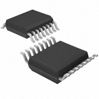
74AC153SC:16引脚小外形集成电路(SOIC)封装,JEDEC MS-012标准,0.150"窄体。 - 74AC153SJ:16引脚小外形封装(SOP),EIAJ TYPE II标准,5.3mm宽。 - 74AC153MTC:16引脚薄型缩减型小外形封装(TSSOP),JEDEC MO-153标准,4.4mm宽。 - 74AC153PC:16引脚塑料双列直插封装(PDIP),JEDEC MS-001标准,0.300"宽。 - 74ACT153SC:与74AC153SC相同封装。 - 74ACT153MTC:与74AC153MTC相同封装。

### 器件简介 74AC153和74ACT153是高速双4输入多路选择器,具有共同的选择输入和每个部分单独的使能输入。它们可以从四个源中选择两条数据线,并且两个缓冲输出呈现的数据为真值(非反相)形式。除了多路选择器操作外,AC/ACT153还可以作为函数发生器,生成任意两个三变量函数。

### 引脚分配 - l0a-3a:A边数据输入。 - lob-l3b:B边数据输入。 - So, S1:共同选择输入。 - Ea, Eb:A边和B边的使能输入。 - za, zb:A边和B边的输出。

### 参数特性 - TTL兼容输入:74ACT153具有TTL兼容输入。 - 输出电流:输出源/汇电流减少50%,可达到24mA。

### 功能详解 AC/ACT153是一个双4输入多路选择器,可以根据共同的选择输入(S0, S1)从多达四个源中选择两个数据位。每个4输入多路选择器电路都有单独的低电平有效的使能(E),可以用来独立控制输出。当使能为高电平时,对应的输出被强制为低电平。

### 应用信息 AC/ACT153可以作为2极4位开关的逻辑实现,其中开关的位置由选择输入提供的逻辑电平决定。

### 封装信息 提供的信息包括SOIC、SOP、TSSOP和PDIP等多种封装类型,具体尺寸和标准在文档中有详细描述和图示。
74ACT153MTC 价格&库存

很抱歉,暂时无法提供与“74ACT153MTC”相匹配的价格&库存,您可以联系我们找货

免费人工找货