74ACTQ00SC

74ACTQ00SC

  • 厂商:

    FAIRCHILD(仙童半导体)

  • 封装:

  • 描述:

    74ACTQ00SC - Quiet Series™Quad 2-Input NAND Gate - Fairchild Semiconductor

  • 详情介绍
  • 数据手册
  • 价格&库存
74ACTQ00SC 数据手册
74ACTQ00 Quiet Series™ Quad 2-Input NAND Gate August 1990 Revised April 1999 74ACTQ00 Quiet Series™ Quad 2-Input NAND Gate General Description The ACTQ00 contains four 2-input NAND gates and utilizes Fairchild FACT Quiet Series™ technology to guarantee quiet output switching and improve dynamic threshold performance FACT Quiet Series features GTO™ output control and undershoot corrector in addition to a split ground bus for superior ACMOS performance. Features s ICC reduced by 50% s Guaranteed simultaneous switching noise level and dynamic threshold performance s Improved latch-up immunity s Outputs source/sink 24 mA s Has TTL-compatible inputs Ordering Code: Order Number 74ACTQ00SC 74ACTQ00PC Package Number M14A N14A Package Description 14-Lead Small Outline Integrated Circuit (SOIC), JEDEC MS-120, 0.150” Narrow Body 14-Lead Plastic Dual-In-Line Package (PDIP), JEDEC MS-001, 0.300” Wide Device also available in Tape and Reel. Specify by appending suffix letter “X” to the ordering code. Logic Symbol IEEE/IEC Connection Diagram Pin Assignment for DIP and SOIC Pin Descriptions Pin Names An, Bn On Description Inputs Outputs FACT™, Quiet Series™, FACT Quiet Series™, and GTO™ are trademarks of Fairchild Semiconductor Corporation. © 1999 Fairchild Semiconductor Corporation DS010888.prf www.fairchildsemi.com 74ACTQ00 Absolute Maximum Ratings(Note 1) Supply Voltage (VCC) DC Input Diode Current (IIK) VI = −0.5V VI = VCC + 0.5V DC Input Voltage (VI) DC Output Diode Current (IOK) VO = −0.5V VO = VCC + 0.5V DC Output Voltage (VO) DC Output Source or Sink Current (IO) DC VCC or Ground Current per Output Pin (ICC or IGND) Storage Temperature (TSTG) ±50 mA −65°C to +150°C ±50 mA −20 mA +20 mA −0.5V to VCC + 0.5V −20 mA +20 mA −0.5V to VCC + 0.5V −0.5V to +7.0V DC Latch-up Source or Sink Current Junction Temperature (TJ) PDIP 140°C ±300 mA Recommended Operating Conditions Supply Voltage (VCC) Input Voltage (VI) Output Voltage (VO) Operating Temperature (TA) Minimum Input Edge Rate (∆V/∆t) VIN from 0.8V to 2.0V VCC @ 4.5V, 5.5V Note 1: Absolute maximum ratings are those values beyond which damage to the device may occur. The databook specifications should be met, without exception, to ensure that the system design is reliable over its power supply, temperature, and output/input loading variables. Fairchild does not 4.5V to 5.5V 0V to VCC 0V to VCC −40°C to +85°C 125 mV/ns DC Electrical Characteristics Symbol VIH VIL VOH Parameter Minimum HIGH Level Input Voltage Maximum LOW Level Input Voltage Minimum HIGH Level Output Voltage VCC (V) 4.5 5.5 4.5 5.5 4.5 5.5 4.5 5.5 VOL Maximum LOW Level Output Voltage 4.5 5.5 4.5 5.5 IIN ICCT IOLD IOHD ICC VOLP VOLV VIHD VILD Maximum Input Leakage Current Maximum ICC/Input Minimum Dynamic Output Current (Note 3) Maximum Quiescent Supply Current Quiet Output Maximum Dynamic VOL Quiet Output Minimum Dynamic VOL Minimum HIGH Level Dynamic Input Voltage Maximum LOW Level Dynamic Input Voltage 5.0 5.0 1.9 1.2 2.2 0.8 V V 5.0 −0.6 −1.2 V 5.5 5.5 5.5 5.5 5.5 5.0 1.1 2.0 1.5 0.6 0.001 0.001 TA = +25°C Typ 1.5 1.5 1.5 1.5 4.49 5.49 2.0 2.0 0.8 0.8 4.4 5.4 3.86 4.86 0.1 0.1 0.36 0.36 ±0.1 TA = −40°C to +85°C Guaranteed Limits 2.0 2.0 0.8 0.8 4.4 5.4 VIN = VIL or VIH 3.76 4.76 0.1 0.1 VIN = VIL or VIH 0.44 0.44 ±1.0 1.5 75 −75 20.0 V µA mA mA mA µA V IOL = 24 mA IOL = 24 mA (Note 2) VI = VCC, GND V I = VCC − 2.1V VOLD = 1.65V Max VOHD = 3.85V Min VIN = VCC or GND Figure 1, Figure 2 (Note 4)(Note 5) Figure 1, Figure 2 (Note 4)(Note 5) (Note 4)(Note 6) (Note 4)(Note 6) V V IOH = −24 mA IOH = −24 mA (Note 2) IOUT = 50 µA V V V VOUT = 0.1V or VCC − 0.1V VOUT = 0.1V or VCC − 0.1V IOUT = −50 µA Units Conditions Note 2: All outputs loaded; thresholds on input associated with output under test. Note 3: Maximum test duration 2.0 ms, one output loaded at a time. Note 4: DIP package. Note 5: Max number of outputs defined as (n). Data inputs are 0V to 3V. One output @ GND. Note 6: Max number of data inputs (n) switching. (n−1) inputs switching 0V to 3V. Input-under-test switching: 3V to threshold (VILD), 0V to threshold (VIHD), f = 1 MHz. www.fairchildsemi.com 2 74ACTQ00 AC Electrical Characteristics VCC Symbol tPLH tPHL tOSHL tOSLH Parameter Propagation Delay Data to Output Propagation Delay Data to Output Output to Output Skew (Note 8) 5.0 0.5 1.0 1.0 ns 5.0 2.0 7.5 2.0 8.0 ns (V) (Note 7) 5.0 Min 2.0 TA = +25°C CL = 50 pF Typ Max 7.5 TA = −40°C to +85°C CL = 50 pF Min 2.0 Max 8.0 ns Units Note 7: Voltage Range 5.0 is 5.0V ±0.5V. Note 8: Skew is defined as the absolute value of the difference between the actual propagation delay for any two separate outputs of the same device. The specification applies to any outputs switching in the same direction, either HIGH to LOW (tOSHL) or LOW to HIGH (tOSLH). Parameter guaranteed by design. Capacitance Symbol CIN CPD Parameter Input Capacitance Power Dissipation Capacitance Typ 4.5 74 Units pF pF VCC = OPEN VCC = 5.0V Conditions 3 www.fairchildsemi.com 74ACTQ00 FACT™ Noise Characteristics The setup of a noise characteristics measurement is critical to the accuracy and repeatability of the tests. The following is a brief description of the setup used to measure the noise characteristics of FACT. Equipment: Hewlett Packard Model 8180A Word Generator PC-163A Test Fixture Tektronics Model 7854 Oscilloscope Procedure: 1. Verify Test Fixture Loading: Standard Load 50 pF, 500Ω. 2. Deskew the HFS generator so that no two channels have greater than 150 ps skew between them. This requires that the oscilloscope be deskewed first. It is important to deskew the word generator channels before testing. This will ensure that the outputs switch simultaneously. 3. Terminate all inputs and outputs to ensure proper loading of the outputs and that the input levels are at the correct voltage. 4. Set the HFS generator to toggle all but one output at a frequency of 1 MHz. Greater frequencies will increase DUT heating and effect the results of the measurement. 5. Set the HFS generator input levels at 0V LOW and 3V HIGH for ACT devices and 0V LOW and 5V HIGH for AC devices. Verify levels with an oscilloscope VOLP/VOLV and VOHP/VOHV: • Determine the quiet output pin that demonstrates the greatest noise levels. The worst case pin will usually be the furthest from the ground pin. Monitor the output voltages using a 50Ω coaxial cable plugged into a standard SMB type connector on the test fixture. Do not use an active FET probe. • Measure VOLP and VOLV on the quiet output during the worst case transition for active and enable. Measure VOHP and VOHV on the quiet output during the worst case active and enable transition. • Verify that the GND reference recorded on the oscilloscope has not drifted to ensure the accuracy and repeatability of the measurements. VILD and VIHD: • Monitor one of the switching outputs using a 50Ω coaxial cable plugged into a standard SMB type connector on the test fixture. Do not use an active FET probe. • First increase the input LOW voltage level, VIL, until the output begins to oscillate or steps out a min of 2 ns. Oscillation is defined as noise on the output LOW level that exceeds VIL limits, or on output HIGH levels that exceed VIH limits. The input LOW voltage level at which oscillation occurs is defined as VILD. • Next decrease the input HIGH voltage level.V IH until the output begins to oscillate or steps out a mine of 2 ns. Oscillation is defined as noise on the output LOW level that exceeds VIL limits, or on output HIGH levels that exceed VIH limits. The input HIGH voltage level at which oscillation occurs is defined as VIHD. • Verify that the GND reference recorded on the oscilloscope has not drifted to ensure the accuracy and repeatability of the measurements. Note 9: VOHV and VOLP are measured with respect to ground reference. Note 10: Input pulses have the following characteristics: f = 1 MHz, tr = 3 ns, tf = 3 ns, skew < 150 ps. FIGURE 1. Quiet Output Noise Voltage Waveforms FIGURE 2. Simultaneous Switching Test Circuit www.fairchildsemi.com 4 74ACTQ00 Physical Dimensions inches (millimeters) unless otherwise noted 14-Lead Small Outline Integrated Circuit (SOIC), JEDEC MS-120, 0.150” Narrow Body Package Number M14A 5 www.fairchildsemi.com 74ACTQ00 Quiet Series™ Quad 2-Input NAND Gate Physical Dimensions inches (millimeters) unless otherwise noted (Continued) 14-Lead Plastic Dual-In-Line Package (PDIP) JEDEC MS-001, 0.300” Wide Package Number N14A LIFE SUPPORT POLICY FAIRCHILD’S PRODUCTS ARE NOT AUTHORIZED FOR USE AS CRITICAL COMPONENTS IN LIFE SUPPORT DEVICES OR SYSTEMS WITHOUT THE EXPRESS WRITTEN APPROVAL OF THE PRESIDENT OF FAIRCHILD SEMICONDUCTOR CORPORATION. As used herein: 2. A critical component in any component of a life support 1. Life support devices or systems are devices or systems device or system whose failure to perform can be reawhich, (a) are intended for surgical implant into the sonably expected to cause the failure of the life support body, or (b) support or sustain life, and (c) whose failure device or system, or to affect its safety or effectiveness. to perform when properly used in accordance with instructions for use provided in the labeling, can be reasonably expected to result in a significant injury to the www.fairchildsemi.com user. Fairchild does not assume any responsibility for use of any circuitry described, no circuit patent licenses are implied and Fairchild reserves the right at any time without notice to change said circuitry and specifications.
74ACTQ00SC
### 物料型号 - 型号:74ACTQ00 - 订购代码: - 
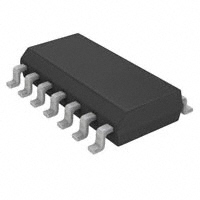
74ACTQ00SC:M14A,14-Lead Small Outline Integrated Circuit (SOIC), JEDEC MS-120, 0.150" Narrow Body - 74ACTQ00PC:N14A,14-Lead Plastic Dual-In-Line Package (PDIP), JEDEC MS-001, 0.300" Wide

### 器件简介 74ACTQ00包含四个2输入NAND门,采用Fairchild FACT Quiet Series™技术,保证安静的输出切换并提高动态阈值性能。该技术具有GTO™输出控制和下冲校正器,以及分割地总线,以实现卓越的ACMOS性能。

### 引脚分配 - An, Bn:输入 - Yn:输出

### 参数特性 - 输出:源/汇24mA - 输入兼容:TTL兼容输入 - 最大直流锁定源/汇电流:±300mA - 结温:PDIP 140°C - 供电电压:-0.5V至+7.0V - 直流输入二极管电流:V=-0.5V时-20mA,VI=Vc+0.5V时+20mA - 直流输入电压:-0.5V至Vcc+0.5V - 直流输出二极管电流:Vo=Vcc+0.5V时+20mA - 直流输出电压:-0.5V至Vcc+0.5V - 直流输出源或汇电流:±50mA - 直流Vcc或地电流每输出引脚:±50mA - 存储温度:-65°C至+150°C

### 功能详解 74ACTQ00是一个四2输入NAND门集成电路,采用FACT Quiet Series技术,具有GTO输出控制和下冲校正器,以及分割地总线,以实现卓越的ACMOS性能。该器件适用于需要安静输出切换和提高动态阈值性能的应用。

### 应用信息 该器件适用于需要低噪声输出和高动态阈值性能的应用,如数字逻辑电路、计算机系统和通信设备。

### 封装信息 - SOIC封装:14-Lead Small Outline Integrated Circuit (SOIC), JEDEC MS-120, 0.150" Narrow Body - PDIP封装:14-Lead Plastic Dual-In-Line Package (PDIP), JEDEC MS-001, 0.300" Wide
74ACTQ00SC 价格&库存

很抱歉,暂时无法提供与“74ACTQ00SC”相匹配的价格&库存,您可以联系我们找货

免费人工找货