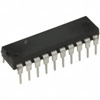
74F373PC

74F373PC

  • 厂商:

    FAIRCHILD(仙童半导体)

  • 封装:

  • 描述:

    74F373PC - Octal Transparent Latch with 3-STATE Outputs - Fairchild Semiconductor

  • 详情介绍
  • 数据手册
  • 价格&库存
74F373PC 数据手册
74F373 Octal Transparent Latch with 3-STATE Outputs May 1988 Revised September 2000 74F373 Octal Transparent Latch with 3-STATE Outputs General Description The 74F373 consists of eight latches with 3-STATE outputs for bus organized system applications. The flip-flops appear transparent to the data when Latch Enable (LE) is HIGH. When LE is LOW, the data that meets the setup times is latched. Data appears on the bus when the Output Enable (OE) is LOW. When OE is HIGH the bus output is in the high impedance state. Features s Eight latches in a single package s 3-STATE outputs for bus interfacing s Guaranteed 4000V minimum ESD protection Ordering Code: Order Number 74F373SC 74F373SJ 74F373MSA 74F373PC Package Number M20B M20D MSA20 N20A Package Description 20-Lead Small Outline Integrated Circuit (SOIC), JEDEC MS-013, 0.300 Wide 20-Lead Small Outline Package (SOP), EIAJ TYPE II, 5.3mm Wide 20-Lead Shrink Small Outline Package (SSOP), EIAJ TYPE II, 5.3mm Wide 20-Lead Plastic Dual-In-Line Package (PDIP), JEDEC MS-001, 0.300 Wide Devices also available in Tape and Reel. Specify by appending the suffix letter “X” to the ordering code. Logic Symbols Connection Diagram IEEE/IEC © 2000 Fairchild Semiconductor Corporation DS009523 www.fairchildsemi.com 74F373 Unit Loading/Fan Out Pin Names D0–D7 LE OE O0–O7 Data Inputs Latch Enable Input (Active HIGH) Output Enable Input (Active LOW) 3-STATE Latch Outputs Description U.L. HIGH/LOW 1.0/1.0 1.0/1.0 1.0/1.0 150/40 (33.3) Input IIH/IIL Output IOH/IOL 20 µA/−0.6 mA 20 µA/−0.6 mA 20 µA/−0.6 mA −3 mA/24 mA (20 mA) Functional Description The 74F373 contains eight D-type latches with 3-STATE output buffers. When the Latch Enable (LE) input is HIGH, data on the Dn inputs enters the latches. In this condition the latches are transparent, i.e., a latch output will change state each time its D input changes. When LE is LOW, the latches store the information that was present on the D inputs a setup time preceding the HIGH-to-LOW transition of LE. The 3-STATE buffers are controlled by the Output Enable (OE) input. When OE is LOW, the buffers are in the bi-state mode. When OE is HIGH the buffers are in the high impedance mode but this does not interfere with entering new data into the latches. Truth Table Inputs LE H H L X OE L L L H Dn H L X X Output On H L On (no change) Z H = H IGH Voltage Level L = LOW Voltage Level X = Immaterial Z = High Impedance State Logic Diagram Please note that this diagram is provided only for the understanding of logic operations and should not be used to estimate propagation delays. www.fairchildsemi.com 2 74F373 Absolute Maximum Ratings(Note 1) Storage Temperature Ambient Temperature under Bias Junction Temperature under Bias VCC Pin Potential to Ground Pin Input Voltage (Note 2) Input Current (Note 2) Voltage Applied to Output in HIGH State (with VCC = 0V) Standard Output 3-STATE Output Current Applied to Output in LOW State (Max) ESD Last Passing Voltage (Min) twice the rated IOL (mA) 4000V −65°C to +150°C −55°C to +125°C −55°C to +150°C −0.5V to +7.0V −0.5V to +7.0V −30 mA to +5.0 mA Recommended Operating Conditions Free Air Ambient Temperature Supply Voltage 0°C to +70°C +4.5V to +5.5V −0.5V to VCC −0.5V to +5.5V Note 1: Absolute maximum ratings are values beyond which the device may be damaged or have its useful life impaired. Functional operation under these conditions is not implied. Note 2: Either voltage limit or current limit is sufficient to protect inputs. DC Electrical Characteristics Symbol VIH VIL VCD VOH Parameter Input HIGH Voltage Input LOW Voltage Input Clamp Diode Voltage Output HIGH Voltage 10% VCC 10% VCC 5% VCC 5% VCC VOL IIH IBVI ICEX VID IOD IIL IOZH IOZL IOS IZZ ICCZ Output LOW Voltage Input HIGH Current Input HIGH Current Breakdown Test Output HIGH Leakage Current Input Leakage Test Output Leakage Circuit Current Input LOW Current Output Leakage Current Output Leakage Current Output Short-Circuit Current Bus Drainage Test Power Supply Current 38 −60 4.75 3.75 −0.6 50 −50 −150 500 55 10% VCC 2.5 2.4 2.7 2.7 0.5 5.0 7.0 50 V µA µA µA V µA mA µA µA mA µA mA Min Max Max Max 0.0 0.0 Max Max Max Max 0.0V Max V Min Min 2.0 0.8 −1.2 Typ Max Units V V V Min VCC Conditions Recognized as a HIGH Signal Recognized as a LOW Signal IIN = −18 mA IOH = −1 mA IOH = −3 mA IOH = −1 mA IOH = −3 mA IOL = 24 mA VIN = 2.7V VIN = 7.0V VOUT = VCC IID = 1.9 µA All Other Pins Grounded VIOD = 150 mV All Other Pins Grounded VIN = 0.5V VOUT = 2.7V VOUT = 0.5V VOUT = 0V VOUT = 5.25V VO = HIGH Z 3 www.fairchildsemi.com 74F373 AC Electrical Characteristics TA = +25°C Symbol Parameter Min tPLH tPHL tPLH tPHL tPZH tPZL tPHZ tPLZ Output Disable Time Propagation Delay Dn to On Propagation Delay LE to On Output Enable Time 3.0 2.0 5.0 3.0 2.0 2.0 1.5 1.5 VCC = +5.0V CL = 50 pF Typ 5.3 3.7 9.0 5.2 5.0 5.6 4.5 3.8 Max 7.0 5.0 11.5 7.0 11.0 7.5 6.5 5.0 TA = −55°C to +125°C VCC = +5.0V CL = 50 pF Min 3.0 2.0 5.0 3.0 2.0 2.0 1.5 1.5 Max 8.5 7.0 15.0 8.5 13.5 10.0 10.0 7.0 TA = 0°C to +70°C VCC = +5.0V CL = 50 pF Min 3.0 2.0 5.0 3.0 2.0 2.0 1.5 1.5 Max 8.0 6.0 13.0 8.0 12.0 8.5 7.5 6.0 ns ns ns ns Units AC Operating Requirements TA = +25°C Symbol Parameter VCC = +5.0V Min tS(H) tS(L) tH(H) tH(L) tW(H) Setup Time, HIGH or LOW Dn to LE Hold Time, HIGH or LOW Dn to LE LE Pulse Width, HIGH 2.0 2.0 3.0 3.0 6.0 Max TA = −55°C to +125°C VCC = +5.0V Min 2.0 2.0 3.0 4.0 6.0 Max TA = 0°C to +70°C VCC = +5.0V Min 2.0 2.0 3.0 3.0 6.0 ns ns Max Units www.fairchildsemi.com 4 74F373 Physical Dimensions inches (millimeters) unless otherwise noted 20-Lead Small Outline Integrated Circuit (SOIC), JEDEC MS-013, 0.300 Wide Package Number M20B 5 www.fairchildsemi.com 74F373 Physical Dimensions inches (millimeters) unless otherwise noted (Continued) 20-Lead Small Outline Package (SOP), EIAJ TYPE II, 5.3mm Wide Package Number M20D www.fairchildsemi.com 6 74F373 Physical Dimensions inches (millimeters) unless otherwise noted (Continued) 20-Lead Shrink Small Outline Package (SSOP), EIAJ TYPE II, 5.3mm Wide Package Number MSA20 7 www.fairchildsemi.com 74F373 Octal Transparent Latch with 3-STATE Outputs Physical Dimensions inches (millimeters) unless otherwise noted (Continued) 20-Lead Plastic Dual-In-Line Package (PDIP), JEDEC MS-001, 0.300 Wide Package Number N20A Fairchild does not assume any responsibility for use of any circuitry described, no circuit patent licenses are implied and Fairchild reserves the right at any time without notice to change said circuitry and specifications. LIFE SUPPORT POLICY FAIRCHILD’S PRODUCTS ARE NOT AUTHORIZED FOR USE AS CRITICAL COMPONENTS IN LIFE SUPPORT DEVICES OR SYSTEMS WITHOUT THE EXPRESS WRITTEN APPROVAL OF THE PRESIDENT OF FAIRCHILD SEMICONDUCTOR CORPORATION. As used herein: 1. Life support devices or systems are devices or systems which, (a) are intended for surgical implant into the body, or (b) support or sustain life, and (c) whose failure to perform when properly used in accordance with instructions for use provided in the labeling, can be reasonably expected to result in a significant injury to the user. www.fairchildsemi.com 8 2. A critical component in any component of a life support device or system whose failure to perform can be reasonably expected to cause the failure of the life support device or system, or to affect its safety or effectiveness. www.fairchildsemi.com
74F373PC
物料型号: - 74F373SC:20引脚小外形集成电路(SOIC),JEDEC MS-013,0.300宽 - 74F373SJ:20引脚小外形封装(SOP),EIAJ TYPE II,5.3mm宽 - 74F373MSA:20引脚缩减型小外形封装(SSOP),EIAJ TYPE II,5.3mm宽 - 74F373PC:20引脚塑料双列直插封装(PDIP),JEDEC MS-001,0.300宽

器件简介: 74F373由八个锁存器组成,具有三态输出,适用于总线组织系统应用。当锁存使能(LE)为高电平时,数据在锁存器中透明;当LE为低电平时,满足设置时间的数据被锁存。当输出使能(OE)为低电平时,数据出现在总线上;当OE为高电平时,总线输出处于高阻抗状态。

引脚分配: - Do-D7:数据输入 - LE:锁存使能输入(高电平有效) - OE:输出使能输入(低电平有效) - 00-07:三态锁存器输出

参数特性: - 输入高电平电压(VIH):最小2.0V - 输入低电平电压(VIL):最大0.8V - 输出高电平电压(VOH):最小2.5V - 输出低电平电压(VaL):最大0.5V - ESD保护:最小4000V

功能详解: 74F373包含八个D型锁存器和三态输出缓冲器。当LE输入为高电平时,Dn输入的数据进入锁存器,在这种状态下锁存器是透明的。当LE为低电平时,锁存器存储在LE从高到低转变之前的设定时间的数据。三态缓冲器由OE输入控制。

应用信息: 74F373适用于需要锁存数据和三态输出缓冲器的总线组织系统。

封装信息: - SOIC封装:M20B - SOP封装:M20D - SSOP封装:MSA20 - PDIP封装:N20A
74F373PC 价格&库存

很抱歉,暂时无法提供与“74F373PC”相匹配的价格&库存,您可以联系我们找货

免费人工找货