74F579PC

74F579PC

  • 厂商:

    FAIRCHILD(仙童半导体)

  • 封装:

  • 描述:

    74F579PC - 8-Bit Bidirectional Binary Counter with 3-STATE Outputs - Fairchild Semiconductor

  • 详情介绍
  • 数据手册
  • 价格&库存
74F579PC 数据手册
74F579 8-Bit Bidirectional Binary Counter with 3-STATE Outputs April 1988 Revised October 2000 74F579 8-Bit Bidirectional Binary Counter with 3-STATE Outputs General Description The 74F579 is a fully synchronous 8-stage up/down counter with multiplexed 3-STATE I/O ports for bus-oriented applications. It features a preset capability for programmable operation, carry lookahead for easy cascading and a U/D input to control the direction of counting. All state changes, whether in counting or parallel loading, are initiated by the rising edge of the clock. Features s Multiplexed 3-STATE I/O ports s Built-in lookahead carry capability s Count frequency 100 MHz typical s Supply current 75 mA typical s Guaranteed 4000V minimum ESD protection Ordering Code: Order Number 74F579SC 74F579SJ 74F579PC Package Number M20B M20D N20A Package Description 20-Lead Small Outline Integrated Circuit (SOIC), JEDEC MS-013, 0.300" Wide 20-Lead Small Outline Package (SOP), EIAJ TYPE II, 5.3mm Wide 20-Lead Plastic Dual-In-Line Package (PDIP), JEDEC MS-001, 0.300 Wide Devices also available in Tape and Reel. Specify by appending the suffix letter “X” tot he ordering code. Logic Symbol Connection Diagram © 2000 Fairchild Semiconductor Corporation DS009568 www.fairchildsemi.com 74F579 Unit Loading/Fan Out Pin Names I/O0–I/O7 PE U/D MR SR CEP CET CS OE CP TC Data Inputs or 3-STATE Outputs Parallel Enable Input (Active LOW) Up-Down Count Control Input Master Reset Input (Active LOW) Synchronous Reset Input (Active LOW) Count Enable Parallel Input (Active LOW) Count Enable Trickle Input (Active LOW) Chip Select Input Active (Active LOW) Output Enable Input (Active LOW) Clock Pulse Input (Active Rising Edge) Terminal Count Output (Active LOW) Description U.L. HIGH/LOW 3.5/0.333 75/15 0.25/0.333 0.25/0.333 0.25/0.333 0.25/0.333 0.25/0.333 0.25/0.333 0.25/0.333 0.25/0.333 0.25/0.333 25/12.5 Input IIH/IIL Output IOH/IOL 70 µA/−0.2 mA −3 mA/24 mA 5 µA/−0.2 mA 5 µA/−0.2 mA 5 µA/−0.2 mA 5 µA/−0.2 mA 5 µA/−0.2 mA 5 µA/−0.2 mA 5 µA/−0.2 mA 5 µA/−0.2 mA 5 µA/−0.2 mA −1 mA/5 mA Function Table MR X X X L H H H H H H SR X X X X L H H H H H CS H L L X X L PE X H H X X L CEP CET U/D X X X X X X H X L L X X X X X X X H L L X X X X X X X X H L OE X H L X X X X X X X CP X X X Function I/Oa to I/Oh in High Z (PE Disabled) I/Oa to I/Oh in High Z Flip-Flop Outputs Appear on I/O Lines Asynchronous Reset for all Flip-Flops Synchronous Reset for all Flip-Flops Parallel Load all Flip-Flops Hold Hold (TC Held HIGH) Count Up Count Down (Not LL) (Not LL) (Not LL) (Not LL) H = HIGH Voltage Level L = LOW Voltage Level X = Immaterial = LOW to HIGH Clock Transition Not LL = CS and PE should never both be LOW voltage level at the same time.       X  www.fairchildsemi.com 2 74F579 Logic Diagrams Please note that this diagram is provided only for the understanding of logic operations and should not be used to estimate propagation delays. VCC = Pin 16 GND = Pin 6 () = Pin Numbers Detail A 3 www.fairchildsemi.com 74F579 Absolute Maximum Ratings(Note 1) Storage Temperature Ambient Temperature under Bias Junction Temperature under Bias VCC Pin Potential to Ground Pin Input Voltage (Note 2) Input Current (Note 2) Voltage Applied to Output in HIGH State (with VCC = 0V) Standard Output 3-STATE Output Current Applied to Output in LOW State (Max) ESD Last Passing Voltage (Min) twice the rated IOL (mA) 4000V −65°C to +150 °C −55°C to +125 °C −55°C to +150 °C −0.5V to +7.0V −0.5V to +7.0V −30 mA to +5.0 mA Recommended Operating Conditions Free Air Ambient Temperature Supply Voltage 0°C to +70°C +4.5V to +5.5V −0.5V to VCC −0.5V to +5.5V Note 1: Absolute maximum ratings are values beyond which the device may be damaged or have its useful life impaired. Functional operation under these conditions is not implied. Note 2: Either voltage limit or current limit is sufficient to protect inputs. DC Electrical Characteristics Symbol VIH VIL VCD VOH Parameter Input HIGH Voltage Input LOW Voltage Input Clamp Diode Voltage Output HIGH Voltage VOL IIH IBVI IBVIT ICEX VID IOD IZZ IIL IIH & IOZH IIL & IOZL IOS ICCH ICCL ICCZ Output LOW Voltage Input HIGH Current Input HIGH Current Breakdown Test Input HIGH Current Breakdown (I/O) Output HIGH Leakage Current Input Leakage Test Output Leakage Circuit Control Bus Drainage Test Input LOW Current Output Leakage Current Output Leakage Current Output Short-Circuit Current Power Supply Current Power Supply Current Power Supply Current −60 70 85 85 4.75 3.75 500 −0.2 70 −200 −150 110 120 125 10% VCC 5% VCC 10% VCC 5% VCC 2.4 2.7 0.5 0.5 5.0 7.0 0.5 50 Min 2.0 0.8 −1.2 Typ Max Units V V V V Min Min VCC Conditions Recognized as a HIGH Signal Recognized as a LOW Signal IIN = −18 mA IOH = −3 mA IOL = 20 mA (TC), IOL = 24 mA (I/On) IOL = 20 mA (TC), IOL = 24 mA (I/On) VIN = 2.7V (Non-I/O Pins) VIN = 7.0V (Non-I/O Pins) VIN = 5.5V (I/On) VOUT = VCC IID = 1.9 µA All Other Pins Grounded VIOD = 150 mV All Other Pins Grounded VOUT = 5.25V VIN = 0.5V (Non-I/O Pins) VOUT = 2.7V (I/On) VOUT = 0.5V (I/On) VOUT = 0V VO = HIGH VO = LOW VO = HIGH Z V µA µA mA µA V µA µA mA µA µA mA mA mA mA Min Max Max Max Max 0.0 0.0 0.0 Max Max Max Max Max Max Max www.fairchildsemi.com 4 74F579 AC Electrical Characteristics TA = +25°C Symbol Parameter Min fMAX tPLH tPHL tPLH tPHL tPLH tPHL tPLH tPHL tPHL tPHL tPZH tPZL tPHZ tPLZ tPZH tPZL tPHZ tPLZ Maximum Clock Frequency Propagation Delay CP to I/On Propagation Delay CP to TC Propagation Delay U/D to TC Propagation Delay CEP or CET to TC Propagation Delay MR to I/On Propagation Delay MR to TC Output Enable Time CS or PE to I/O Output Disable Time CS or PE to I/O Output Enable Time OE to I/On Output Disable Time OE to I/On 70 3.0 5.0 5.0 5.0 4.5 4.5 2.5 3.5 5.0 6.5 3.0 5.5 2.0 2.0 3.0 5.0 2.0 2.0 VCC = +5.0V CL = 50 pF Typ 85 5.0 8.0 7.5 7.0 7.0 8.0 3.8 6.0 7.5 10.0 5.0 8.0 5.0 4.5 5.0 8.0 4.0 4.0 7.5 11.5 11.5 11.5 9.0 9.5 6.0 8.0 10.0 13.0 8.5 10.5 8.5 8.0 8.0 11.0 6.5 6.0 Max TA = 0°C to +70°C VCC = +5.0V CL = 50 pF Min 80 3.0 5.0 5.0 5.0 4.5 4.5 2.5 3.5 5.0 6.5 3.0 5.5 2.0 2.0 3.0 5.0 2.0 2.0 8.0 11.5 12.0 12.0 10.0 10.0 6.5 8.5 10.0 13.5 9.0 11.5 9.0 8.5 8.5 12.0 6.5 6.5 ns ns ns ns ns ns ns ns ns ns Max Units AC Operating Requirements TA = +25°C Symbol Parameter Min tS(H) tS(L) tH(H) tH(L) tS(H) tS(L) tH(H) tH(L) tS(H) tS(L) tH(H) tH(L) tS(H) tS(L) tH(H) tH(L) tW(H) tW(L) tW(L) tREC Setup Time I/On to CP Hold Time I/On to CP Setup Time PE, CS or SR to CP Hold Time PE, CS or SR to CP Setup Time CET or CEP to CP Hold Time CET or CEP to CP Setup Time U/D to CP Hold Time U/D to CP Clock Pulse Width HIGH or LOW MR Pulse Width Recovery Time MR to CP 4.0 4.0 0.0 0.0 9.5 9.5 0.0 0.0 6.5 9.5 0.0 0.0 9.0 9.0 0.0 0.0 4.5 4.5 3.0 4.0 VCC = +5.0V Typ Max TA = 0°C to +70°C VCC = +5.0V Min 4.0 4.0 0.0 0.0 9.5 9.5 0.0 0.0 6.5 9.5 0.0 0.0 9.5 9.5 0.0 0.0 4.5 4.5 3.0 4.0 Max ns ns ns ns ns ns ns ns ns ns ns Units 5 www.fairchildsemi.com 74F579 Physical Dimensions inches (millimeters) unless otherwise noted 20-Lead Small Outline Integrated Circuit (SOIC), JEDEC MS-013, 0.300" Wide Package Number M20B www.fairchildsemi.com 6 74F579 Physical Dimensions inches (millimeters) unless otherwise noted (Continued) 20-Lead Small Outline Package (SOP), EIAJ TYPE II, 5.3mm Wide Package Number M20D 7 www.fairchildsemi.com 74F579 8-Bit Bidirectional Binary Counter with 3-STATE Outputs Physical Dimensions inches (millimeters) unless otherwise noted (Continued) 20-Lead Plastic Dual-In-Line Package (PDIP), JEDEC MS-001, 0.300 Wide Package Number N20A Fairchild does not assume any responsibility for use of any circuitry described, no circuit patent licenses are implied and Fairchild reserves the right at any time without notice to change said circuitry and specifications. LIFE SUPPORT POLICY FAIRCHILD’S PRODUCTS ARE NOT AUTHORIZED FOR USE AS CRITICAL COMPONENTS IN LIFE SUPPORT DEVICES OR SYSTEMS WITHOUT THE EXPRESS WRITTEN APPROVAL OF THE PRESIDENT OF FAIRCHILD SEMICONDUCTOR CORPORATION. As used herein: 1. Life support devices or systems are devices or systems which, (a) are intended for surgical implant into the body, or (b) support or sustain life, and (c) whose failure to perform when properly used in accordance with instructions for use provided in the labeling, can be reasonably expected to result in a significant injury to the user. www.fairchildsemi.com 8 2. A critical component in any component of a life support device or system whose failure to perform can be reasonably expected to cause the failure of the life support device or system, or to affect its safety or effectiveness. www.fairchildsemi.com
74F579PC
### 物料型号 - 74F579SC:20引脚小外形集成电路(SOIC),JEDEC MS-013,0.300"宽 - 74F579SJ:20引脚小外形封装(SOP),EIAJ TYPE II,5.3mm宽 - 
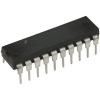
74F579PC:20引脚塑料双列直插式封装(PDIP),JEDEC MS-001,0.300"宽

### 器件简介 74F579是一款完全同步的8级上/下计数器,具有多路复用3态I/O端口,适用于总线导向应用。它具备预置功能以实现可编程操作,进位前瞻功能便于级联,以及U/D输入以控制计数方向。所有状态变化,无论是计数还是并行加载,都由时钟的上升沿触发。

### 引脚分配 - 1-8:数据输入或3态输出 - P:并行使能输入(低电平有效) - U/D:上/下计数控制输入 - MR:主复位输入(低电平有效) - SR:同步复位输入(低电平有效) - CEP/CET:并行使能输入(低电平有效) - CS:芯片选择输入(低电平有效) - OE:输出使能输入(低电平有效) - CP:时钟脉冲输入(上升沿有效) - TC:终端计数输出(低电平有效)

### 参数特性 - 最大计数频率:100MHz(典型值) - 供电电流:75mA(典型值) - ESD保护:保证最小4000V

### 功能详解 74F579具有多路复用3态I/O端口、内置前瞻进位能力、计数频率100MHz、典型供电电流75mA、保证最小4000V的ESD保护。

### 应用信息 适用于需要8位双向计数功能的总线导向应用,如数字显示、计数、寄存器等。

### 封装信息 - SOIC封装:M20B - SOP封装:M20D - PDIP封装:N20A
74F579PC 价格&库存

很抱歉,暂时无法提供与“74F579PC”相匹配的价格&库存,您可以联系我们找货

免费人工找货