74F652SC

74F652SC

  • 厂商:

    FAIRCHILD(仙童半导体)

  • 封装:

  • 描述:

    74F652SC - Transceivers/Registers - Fairchild Semiconductor

  • 详情介绍
  • 数据手册
  • 价格&库存
74F652SC 数据手册
74F651 • 74F652 Transceivers/Registers March 1988 Revised August 1999 74F651 • 74F652 Transceivers/Registers General Description These devices consist of bus transceiver circuits with Dtype flip-flops, and control circuitry arranged for multiplexed transmission of data directly from the input bus or from internal registers. Data on the A or B bus will be clocked into the registers as the appropriate clock pin goes to HIGH logic level. Output Enable pins (OEAB, OEBA) are provided to control the transceiver function. Features s Independent registers for A and B buses s Multiplexed real-time and stored data s Choice of non-inverting and inverting data paths 74F651 inverting 74F652 non-inverting Ordering Code: Order Number 74F651SC 74F651SPC 74F652SC 74F652SPC Package Number M24B N24C M24B N24C Package Description 24-Lead Small Outline Integrated Circuit (SOIC), JEDEC MS-013, 0.300 Wide 24-Lead Plastic Dual-In-Line Package (PDIP), JEDEC MS-100, 0.300 Wide 24-Lead Small Outline Integrated Circuit (SOIC), JEDEC MS-013, 0.300 Wide 24-Lead Plastic Dual-In-Line Package (PDIP), JEDEC MS-100, 0.300 Wide Devices also available in Tape and Reel. Specify by appending the suffix letter “X” to the ordering code. Connection Diagram © 1999 Fairchild Semiconductor Corporation DS009581 www.fairchildsemi.com 74F651 • 74F652 Logic Symbols 74F651 74F652 IEEE/IEC 74F651 IEEE/IEC 74F652 Unit Loading/Fan Out Pin Names A0–A7, B0–B7 CPAB, CPBA SAB, SBA OEAB, OEBA Description A and B Inputs/ 3-STATE Outputs Clock Inputs Select Inputs Output Enable Inputs U.L. HIGH/LOW 1.0/1.0 600/106.6 (80) 1.0/1.0 1.0/1.0 1.0/1.0 Input IIH/IIL Output IOH/IOL 20 µA/−0.6 mA −12 mA/64 mA (48 mA) 20 µA/−0.6 mA 20 µA/−0.6 mA 20 µA/−0.6 mA Function Table Inputs OEAB OEBA CPAB CPBA SAB SBA L L X H L L L L H H H H H H H X L L L H H L H or L H or L H or L Inputs/Outputs (Note 1) A0 thru A7 Input Input Input Output Output Input Output B0 thru B7 Input Operating Mode Isolation Store A and B Data Not Specified Store A, Hold B Output Input Input Output Output Store A in Both Registers Hold A, Store B Store B in Both Registers Real-Time B Data to A Bus Store B Data to A Bus Real-Time A Data to B Bus Stored A Data to B Bus Stored A Data to B Bus and Stored B Data to A Bus H = HIGH Voltage Level L = LOW Voltage Level H or L X     X X     X X X X X X X X X X X L H H X X X X X X L H X X H Not Specified Input H or L H or L H or L H or L  X = Immaterial = LOW-to-HIGH Clock Transition Note 1: The data output functions may be enabled or disabled by various signals at OEAB or OEBA inputs. Data input functions are always enabled, i.e., data at the bus pins will be stored on every LOW-to-HIGH transition on the clock inputs. www.fairchildsemi.com 2 74F651 • 74F652 Functional Description In the transceiver mode, data present at the HIGH impedance port may be stored in either the A or B register or both. The select (SAB, SBA) controls can multiplex stored and real-time. The examples in Figure 1 demonstrate the four fundamental bus-management functions that can be performed with the Octal bus transceivers and receivers. Data on the A or B data bus, or both can be stored in the internal D flip-flop by LOW-to-HIGH transitions at the appropriate Clock Inputs (CPAB, CPBA) regardless of the Select or Output Enable Inputs. When SAB and SBA are in the real time transfer mode, it is also possible to store data without using the internal D flip-flops by simultaneously enabling OEAB and OEBA. In this configuration each Output reinforces its Input. Thus when all other data sources to the two sets of bus lines are in a HIGH impedance state, each set of bus lines will remain at its last state. Note A: Real-Time Transfer Bus B to Bus A Note B: Real-Time Transfer Bus A to Bus B OEAB OEBA CPAB CPBA SAB SBA L L X X X L OEAB OEBA CPAB CPBA SAB SBA H H X X L X Note C: Storage Note D: Transfer Storage Data to A or B OEAB OEBA CPAB CPBA SAB SBA X L L H X H X X X X X X X FIGURE 1. X    OEAB OEBA CPAB CPBA SAB SBA H L H or L H or L H X 3 www.fairchildsemi.com 74F651 • 74F652 Logic Diagrams 74F652 Please note that this diagram is provided only for the understanding of logic operations and should not be used to estimate propagation delays. 74F651 Please note that this diagram is provided only for the understanding of logic operations and should not be used to estimate propagation delays. www.fairchildsemi.com 4 74F651 • 74F652 Absolute Maximum Ratings(Note 2) Storage Temperature Ambient Temperature under Bias Junction Temperature under Bias VCC Pin Potential to Ground Pin Input Voltage (Note 3) Input Current (Note 3) Voltage Applied to Output in HIGH State (with VCC = 0V) Standard Output 3-STATE Output Current Applied to Output in LOW State (Max) ESD Last Passing Voltage (Min) twice the rated IOL (mA) 4000V −0.5V to VCC −0.5V to +5.5V −65°C to +150°C −55°C to +125°C −55°C to +150°C −0.5V to +7.0V −0.5V to +7.0V −30 mA to +5.0 mA Recommended Operating Conditions Free Air Ambient Temperature Supply Voltage 0°C to +70°C +4.5V to +5.5V Note 2: Absolute maximum ratings are values beyond which the device may be damaged or have its useful life impaired. Functional operation under these conditions is not implied. Note 3: Either voltage limit or current limit is sufficient to protect inputs. DC Electrical Characteristics Symbol VIH VIL VCD VOH VOL IIH IBVI IBVIT ICEX VID IOD IIL IIH + IOZH IIL + IOZL IOS IZZ ICCH ICCL ICCZ Parameter Input HIGH Voltage Input LOW Voltage Input Clamp Diode Voltage Output HIGH Voltage Output LOW Voltage Input HIGH Current Input HIGH Current Breakdown Test Input HIGH Current Breakdown (I/O) Output HIGH Leakage Current Input Leakage Test Output Leakage Circuit Current Input LOW Current Output Leakage Current Output Leakage Current Output Short-Circuit Current Bus Drainage Test Power Supply Current Power Supply Current Power Supply Current 105 118 115 −100 4.75 3.75 −0.6 70 −650 −225 500 135 150 150 10% VCC 10% VCC 2.0 0.55 5.0 7.0 0.5 50 Min 2.0 0.8 −1.2 Typ Max Units V V V V V µA µA mA µA V µA mA µA µA mA µA mA mA mA Min Min Min Max Max Max Max 0.0 0.0 Max Max Max Max 0.0V Max Max Max VCC Conditions Recognized as a HIGH Signal Recognized as a LOW Signal IIN = −18 mA (Non I/O Pins) IOH = −15 mA (An, Bn) IOL = 64 mA (A n, Bn) VIN = 2.7V (Non I/O Pins) VIN = 7.0V VIN = 5.5V (An, Bn) VOUT = VCC IID = 1.9 µA All Other Pins Grounded VIIOD = 150 mV All Other Pins Grounded VIN = 0.5V (Non I/O Pins) VOUT = 2.7V (An, Bn) VOUT = 0.5V (An, Bn) VOUT = 0V VOUT = 5.25V VO = HIGH VO = LOW VO = HIGH Z 5 www.fairchildsemi.com 74F651 • 74F652 AC Electrical Characteristics TA = +25°C Symbol Parameter VCC = +5.0V CL = 50 pF Min fMAX tPLH tPHL tPLH tPHL tPLH tPHL tPLH tPHL Max. Clock Frequency Propagation Delay Clock to Bus Propagation Delay Bus to Bus (74F651) Propagation Delay Bus to Bus (74F652) Propagation Delay SBA or SAB to A or B 90 2.0 2.0 2.0 1.0 1.0 1.0 2.0 2.0 7.0 8.0 8.5 7.5 7.0 6.5 8.5 8.0 Max TA = −55°C to +125°C VCC = +5.0V CL = 50 pF Min 75 2.0 2.0 1.0 1.0 1.0 1.0 2.0 2.0 8.5 9.5 9.0 8.0 8.0 8.0 11.0 10.0 Max TA = 0°C to +70°C VCC = +5.0V CL = 50 pF Min 90 2.0 2.0 2.0 1.0 1.0 1.0 2.0 2.0 8.0 9.0 9.0 8.0 7.5 7.0 9.5 9.0 Max MHz ns ns ns ns Units AC Operating Requirements TA = +25°C Symbol Parameter VCC = +5.0V Min tPZH tPZL tPHZ tPLZ tPZH tPZL tPHZ tPLZ tS(H) tS(L) tH(H) tH(L) tW(H) tW(L) Enable Time *OEBA to A Disable Time *OEBA to A Enable Time OEAB to B Disable Time OEAB to B Setup Time, HIGH or LOW, Bus to Clock Hold Time, HIGH or LOW, Bus to Clock Clock Pulse Width HIGH or LOW 2.0 2.0 1.0 2.0 2.0 3.0 2.0 2.0 5.0 5.0 2.0 2.0 5.0 5.0 Max 9.5 12.0 7.5 8.5 9.5 13.0 9.0 10.5 TA = −55°C to +125°C VCC = +5.0V Min 2.0 2.0 1.0 1.0 2.0 2.0 1.0 1.0 5.0 5.0 2.5 2.5 5.0 5.0 Max 10.0 10.0 9.0 9.0 10.0 12.0 9.0 12.0 TA = 0°C to +70°C VCC = +5.0V Min 2.0 2.0 1.0 2.0 2.0 3.0 2.0 2.0 5.0 5.0 2.0 2.0 5.0 5.0 Max 10.0 12.5 8.0 9.0 10.0 14.0 10.0 11.0 ns ns ns ns ns Units www.fairchildsemi.com 6 74F651 • 74F652 Physical Dimensions inches (millimeters) unless otherwise noted 24-Lead Small Outline Integrated Circuit (SOIC), JEDEC MS-013, 0.300 Wide Package Number M24B 7 www.fairchildsemi.com 74F651 • 74F652 Transceivers/Registers Physical Dimensions inches (millimeters) unless otherwise noted (Continued) 24-Lead Plastic Dual-In-Line Package (PDIP), JEDEC MS-100, 0.300 Wide Package Number N24C Fairchild does not assume any responsibility for use of any circuitry described, no circuit patent licenses are implied and Fairchild reserves the right at any time without notice to change said circuitry and specifications. LIFE SUPPORT POLICY FAIRCHILD’S PRODUCTS ARE NOT AUTHORIZED FOR USE AS CRITICAL COMPONENTS IN LIFE SUPPORT DEVICES OR SYSTEMS WITHOUT THE EXPRESS WRITTEN APPROVAL OF THE PRESIDENT OF FAIRCHILD SEMICONDUCTOR CORPORATION. As used herein: 1. Life support devices or systems are devices or systems which, (a) are intended for surgical implant into the body, or (b) support or sustain life, and (c) whose failure to perform when properly used in accordance with instructions for use provided in the labeling, can be reasonably expected to result in a significant injury to the user. www.fairchildsemi.com 8 2. A critical component in any component of a life support device or system whose failure to perform can be reasonably expected to cause the failure of the life support device or system, or to affect its safety or effectiveness. www.fairchildsemi.com
74F652SC
1. 物料型号: - 
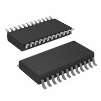
74F651SC:24-Lead Small Outline Integrated Circuit (SOIC), JEDEC MS-013, 0.300 Wide - 74F651SPC:24-Lead Plastic Dual-In-Line Package (PDIP), JEDEC MS-100, 0.300 Wide - 74F652SC:24-Lead Small Outline Integrated Circuit (SOIC), JEDEC MS-013, 0.300 Wide - 74F652SPC:24-Lead Plastic Dual-In-Line Package (PDIP), JEDEC MS-100, 0.300 Wide

2. 器件简介: - 这些设备由总线收发器电路、D型触发器和控制电路组成,用于直接从输入总线或内部寄存器进行数据的多路传输。当相应的时钟引脚变为高电平时,A或B总线上的数据将被时钟进入寄存器。提供输出使能引脚(OEAB, OEBA)来控制收发器功能。

3. 引脚分配: - A0–A7, B0–B7:A和B输入/3态输出 - CPAB, CPBA:时钟输入 - SAB, SBA:选择输入 - OEAB, OEBA:输出使能输入

4. 参数特性: - 独立寄存器用于A和B总线 - 多路复用实时和存储数据 - 选择非反相和反相数据路径 - 74F651为反相,74F652为非反相

5. 功能详解应用信息: - 在收发器模式下,HIGH阻抗端口上的数据可以存储在A或B寄存器中或两者都存储。选择(SAB, SBA)控制可以多路复用存储和实时数据。 - 提供了四个基本总线管理功能的示例,这些功能可以通过八总线收发器和接收器来实现。

6. 封装信息: - SOIC封装:24-Lead Small Outline Integrated Circuit, JEDEC MS-013, 0.300 Wide - PDIP封装:24-Lead Plastic Dual-In-Line Package, JEDEC MS-100, 0.300 Wide
74F652SC 价格&库存

很抱歉,暂时无法提供与“74F652SC”相匹配的价格&库存,您可以联系我们找货

免费人工找货