0
登录后你可以
  • 下载海量资料
  • 学习在线课程
  • 观看技术视频
  • 写文章/发帖/加入社区
会员中心
创作中心
发布
  • 发文章

  • 发资料

  • 发帖

  • 提问

  • 发视频

创作活动
74LCX06M

74LCX06M

  • 厂商:

    FAIRCHILD(仙童半导体)

  • 封装:

  • 描述:

    74LCX06M - Low Voltage Hex Inverter/Buffer with Open Drain Outputs - Fairchild Semiconductor

  • 详情介绍
  • 数据手册
  • 价格&库存
74LCX06M 数据手册
74LCX06 Low Voltage Hex Inverter/Buffer with Open Drain Outputs October 1999 Revised January 2001 74LCX06 Low Voltage Hex Inverter/Buffer with Open Drain Outputs General Description The LCX06 contains six inverters/buffers. The inputs tolerate voltages up to 7V allowing the interface of 5V systems to 3V systems. The outputs of the LCX06 are open drain and can be connected to other open drain outputs to implement active LOW wire AND or active HIGH wire OR functions. The 74LCX06 is fabricated with advanced CMOS technology to achieve high speed operation while maintaining CMOS low power dissipation. Features s 5V tolerant inputs s 2.3V–3.6V VCC specifications provided s 3.7 ns tPD max (VCC = 3.3V), 10 µA ICC max s Power down high impedance inputs and outputs s ±24 mA output drive (VCC = 3.0V) s Implements patented noise/EMI reduction circuitry s Latch-up performance exceeds 500 mA s Functionally compatible with 74 series 05 s ESD performance: Human body model > 2000V Machine model > 200V Ordering Code: Order Number 74LCX06M 74LCX06SJ 74LCX06MTC Package Number M14A M14D MTC14 Package Description 14-Lead Small Outline Integrated Circuit (SOIC), JEDEC MS-012, 0.150 Narrow 14-Lead Small Outline Package (SOP), EIAJ TYPE II, 5.3mm Wide 14-Lead Thin Shrink Small Outline Package (TSSOP), JEDEC MO-153, 4.4mm Wide Devices also available in Tape and Reel. Specify by appending the suffix letter “X” to the ordering code. Logic Symbol IEEE/IEC Connection Diagram Pin Descriptions Pin Names An On Description Inputs Outputs © 2001 Fairchild Semiconductor Corporation DS500237 www.fairchildsemi.com 74LCX06 Absolute Maximum Ratings(Note 1) Symbol VCC VI VO IIK IOK IO ICC IGND TSTG Parameter Supply Voltage DC Input Voltage DC Output Voltage DC Input Diode Current DC Output Diode Current DC Output Source/Sink Current DC Supply Current per Supply Pin DC Ground Current per Ground Pin Storage Temperature Value Conditions Units V V Output in HIGH or LOW State (Note 2) VI < GND VO < GND VO > VCC V mA mA mA mA mA −0.5 to +7.0 −0.5 to +7.0 −0.5 to VCC + 0.5 −50 −50 +50 ±50 ±100 ±100 −65 to +150 (Note 3) Min Operating Data Retention 2.0 1.5 0 HIGH or LOW State VCC = 3.0V − 3.6V VCC = 2.7V − 3.0V VCC = 2.3V − 2.7V 0 Max 3.6 3.6 5.5 VCC °C Recommended Operating Conditions Symbol VCC VI VO IOH/IOL Supply Voltage Input Voltage Output Voltage Output Current Parameter Units V V V mA ±24 ±12 ±8 −40 0 85 10 TA Free-Air Operating Temperature Input Edge Rate, VIN = 0.8V–2.0V, VCC = 3.0V °C ns/V ∆t/∆V Note 1: The Absolute Maximum Ratings are those values beyond which the safety of the device cannot be guaranteed. The device should not be operated at these limits. The parametric values defined in the Electrical Characteristics tables are not guaranteed at the Absolute Maximum Ratings. The “Recommended Operating Conditions” table will define the conditions for actual device operation. Note 2: IO Absolute Maximum Rating must be observed. Note 3: Unused inputs must be held HIGH or LOW. They may not float. DC Electrical Characteristics Symbol VIH VIL VOL Parameter HIGH Level Input Voltage LOW Level Input Voltage LOW Level Output Voltage IOL = −100 µA IOL = 8 mA IOL = 12 mA IOL = 16 mA IOL = 24 mA II IOFF ICC ∆ICC Input Leakage Current Power-Off Leakage Current Quiescent Supply Current Increase in ICC per Input 0 ≤ VI ≤ 5.5V VI or VO = 5.5V VI = V CC or GND 3.6V ≤ VI ≤ 5.5V VIH = VCC −0.6V Conditions VCC (V) 2.3 − 2.7 2.7 − 3.6 2.3 − 2.7 2.7 − 3.6 2.3 − 3.6 2.3 2.7 3.0 3.0 2.3 − 3.6 0 2.3 − 3.6 2.3 − 3.6 2.3 − 3.6 TA = −40°C to +85°C Min 1.7 2.0 0.7 0.8 0.2 0.6 0.4 0.4 0.55 ±5.0 10 10 ±10 500 µA µA µA µA V Max V V Units www.fairchildsemi.com 2 74LCX06 AC Electrical Characteristics TA = −40°C to +85°C, RL = 500Ω Symbol Parameter VCC = 3.3V ± 0.3V CL= 50 pF Min tPZL tPLZ Propagation Delay Time 0.8 0.8 Max 3.7 3.7 VCC = 2.7V CL = 50 pF Min 1.0 1.0 Max 4.1 4.1 VCC = 2.5V ± 0.2V CL= 30 pF Min 0.8 0.8 Max 3.5 3.5 ns Units Note 4: Skew is defined as the absolute value of the difference between the actual propagation delay for any two separate outputs of the same device. The specification applies to any outputs switching in the same direction, either HIGH-to-LOW (tOSHL) or LOW-to-HIGH (tOSLH). Dynamic Switching Characteristics Symbol VOLP VOLV Parameter Quiet Output Dynamic Peak VOL Quiet Output Dynamic Valley VOL Conditions CL = 50 pF, VIH = 3.3V, VIL = 0V CL = 30 pF, VIH = 2.5V, VIL = 0V CL = 50 pF, VIH = 3.3V, VIL = 0V CL = 30 pF, VIH = 2.5V, VIL = 0V VCC (V) 3.3 2.5 3.3 2.5 TA = 25°C Typical 0.9 0.7 −0.8 −0.6 V V Units Capacitance Symbol CIN COUT CPD Input Capacitance Output Capacitance Power Dissipation Capacitance Parameter Conditions VCC = Open, VI = 0V or VCC VCC = 3.3V, VI = 0V or VCC VCC = 3.3V, VI = 0V or VCC, f = 10 MHz Typical 7 8 25 Units pF pF pF 3 www.fairchildsemi.com 74LCX06 AC Loading and Waveforms Generic for LCX Family FIGURE 1. AC Test Circuit (CL includes probe and jig capacitance) Test tPLH, tPHL tPZL, tPLZ tPZH,tPHZ Switch OPEN 6V at VCC = 3.3 ± 0.3V VCC x 2 at VCC = 2.5 ± 0.2V GND 3-STATE Output High Enable and Disable TImes for Logic FIGURE 2. Waveforms trise and tfall (Input Pulse Characteristics; f = 1MHz, t r = tf = 3ns) Symbol Vmi Vmo Vx Vy VCC 3.3V ± 0.3V 1.5V 1.5V VOL + 0.3V VOH − 0.3V 2.7V 1.5V 1.5V VOL + 0.3V VOH − 0.3V 2.5V ± 0.2V VCC/2 VCC/2 VOL + 0.15V VOH − 0.15V www.fairchildsemi.com 4 74LCX06 Physical Dimensions inches (millimeters) unless otherwise noted 14-Lead Small Outline Integrated Circuit (SOIC), JEDEC MS-012, 0.150 Narrow Package Number M14A 5 www.fairchildsemi.com 74LCX06 Physical Dimensions inches (millimeters) unless otherwise noted (Continued) 14-Lead Small Outline Package (SOP), EIAJ TYPE II, 5.3mm Wide Package Number M14D www.fairchildsemi.com 6 74LCX06 Low Voltage Hex Inverter/Buffer with Open Drain Outputs Physical Dimensions inches (millimeters) unless otherwise noted (Continued) 14-Lead Thin Shrink Small Outline Package (TSSOP), JEDEC MO-153, 4.4mm Wide Package Number MTC14 Fairchild does not assume any responsibility for use of any circuitry described, no circuit patent licenses are implied and Fairchild reserves the right at any time without notice to change said circuitry and specifications. LIFE SUPPORT POLICY FAIRCHILD’S PRODUCTS ARE NOT AUTHORIZED FOR USE AS CRITICAL COMPONENTS IN LIFE SUPPORT DEVICES OR SYSTEMS WITHOUT THE EXPRESS WRITTEN APPROVAL OF THE PRESIDENT OF FAIRCHILD SEMICONDUCTOR CORPORATION. As used herein: 1. Life support devices or systems are devices or systems which, (a) are intended for surgical implant into the body, or (b) support or sustain life, and (c) whose failure to perform when properly used in accordance with instructions for use provided in the labeling, can be reasonably expected to result in a significant injury to the user. 7 2. A critical component in any component of a life support device or system whose failure to perform can be reasonably expected to cause the failure of the life support device or system, or to affect its safety or effectiveness. www.fairchildsemi.com www.fairchildsemi.com
74LCX06M
1. 物料型号: - 
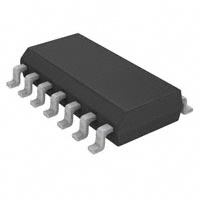
74LCX06M:14-Lead Small Outine Integrated Circuit (SOIC), JEDEC MS-012, 0.150 Narrow - 74LCX06SJ:14-Lead Small Outline Package (SOP), EIAJ TYPE II, 5.3mm Wide - 74LCX06MTC:14-Lead Thin Shrink Small Outline Package (TSSOP), JEDEC MO-153, 4.4mm Wide

2. 器件简介: - 74LCX06包含六个反相器/缓冲器。输入端能承受高达7V的电压,允许5V系统与3V系统之间的接口。 - 输出端为开漏形式,可以连接其他开漏输出以实现主动低线与或主动高线或功能。

3. 引脚分配: - An:输入端 - 0n:输出端

4. 参数特性: - 5V容限输入 - 2.3V–3.6V VCC规格 - 最大3.7ns传播延迟时间 - 电源关闭时高阻抗输入输出 - 专利噪音/EMI降低电路

5. 功能详解: - 74LCX06使用先进的CMOS技术,实现高速操作的同时保持CMOS低功耗特性。 - 与74系列功能兼容,具有超过500mA的抗锁性能。

6. 应用信息: - 该器件适用于需要低电压操作和开漏输出以实现线逻辑功能的应用。

7. 封装信息: - 提供SOIC、SOP和TSSOP三种不同的封装选项,具体尺寸和特性在文档中有详细描述。
74LCX06M 价格&库存

很抱歉,暂时无法提供与“74LCX06M”相匹配的价格&库存,您可以联系我们找货

免费人工找货