1. 物料型号:
- 型号为BCW33,由Fairchild Semiconductor生产。
2. 器件简介:
- BCW33是一款NPN通用放大器,设计用于集电极电流高达300mA的通用应用场合。
3. 引脚分配:
- 1. Base(基极)
- 2. Emitter(发射极)
- 3. Collector(集电极)
4. 参数特性:
- 绝对最大额定值(除非另有说明,Ta=25°C):
- VCEO(集电极-发射极电压):32V
- VCBO(集电极-基极电压):32V
- VEBO(发射极-基极电压):5.0V
- lc(集电极电流(DC)):500mA
- TJ,Tstg(工作和存储结温度范围):-55~+150°C
5. 功能详解:
- 电气特性(Ta=25°C除非另有说明):
- 截止特性:
- V(BR)CBO(集电极-基极击穿电压):32V
- V(BR)CEO(集电极-发射极击穿电压):32V
- V(BR)EBO(发射极-基极击穿电压):5.0V
- CBO(集电极截止电流):100nA(VcB = 32V, Ic = 0)
- 导通特性:
- hFE(直流电流增益):420至800
- VcE(sa)(集电极-发射极饱和电压):0.25V(Ic = 10mA, Ig = 0.5mA)
- VBE(on)(基极-发射极导通电压):0.55至0.7V
- 小信号特性:
- fT(电流增益带宽积):200MHz(Ic= 2.0mA, VCE = 5.0V f=35MHz)
- Cob(输出电容):4.0pF(VcB=10V, Ic=0, f=1.0MHz)
- NF(噪声系数):10dB(Ic = 0.2mA, VCE = 5.0V Rs = 2.0k, f= 1.0kHz Bw= 200Hz)
6. 应用信息:
- 该器件适用于需要NPN晶体管进行信号放大的场合,如音频放大器、开关应用等。
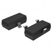
7. 封装信息:
- BCW33采用SOT-23封装,尺寸为40mm × 40mm × 1.5mm。