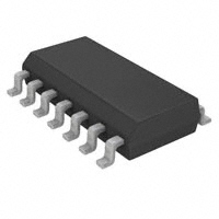
CD4024BC 7-Stage Ripple Carry Binary Counter
October 1987 Revised April 2002
CD4024BC 7-Stage Ripple Carry Binary Counter
General Description
The CD4024BC is a 7-stage ripple-carry binary counter. Buffered outputs are externally available from stages 1 through 7. The counter is reset to its logical “0” stage by a logical “1” on the reset input. The counter is advanced one count on the negative transition of each clock pulse.
Features
s Wide supply voltage range: s Low power TTL compatibility: or 1 driving 74LS s High speed: 12 MHz (typ.) 3.0V to 15V Fan out of 2 driving 74L s High noise immunity: 0.45 VDD (typ.)
input pulse rate VDD − VSS = 10V s Fully static operation
Ordering Code:
Order Number CD4024BCM CD4024BCN Package Number M14A N14A Package Description 14-Lead Small Outline Integrated Circuit (SOIC), JEDEC MS-012, 0.150" Narrow 14-Lead Plastic Dual-In-Line Package (PDIP), JEDEC MS-001, 0.300" Wide
Devices also available in Tape and Reel. Specify by appending the suffix letter “X” to the ordering code.
Connection Diagram
Top View
© 2002 Fairchild Semiconductor Corporation
DS005957
www.fairchildsemi.com
�CD4024BC
Logic Diagrams
Input Logic
Flip-flop logic (1 of 7 identical stages).
Block Diagram
www.fairchildsemi.com
2
�CD4024BC
Absolute Maximum Ratings(Note 1)
(Note 2) DC Supply Voltage (VDD) Input Voltage (VIN ) Storage Temperature Range (TS) Power Dissipation (PD) Dual-In-Line Small Outline Lead Temperature (Soldering, 10 seconds) (TL) 260°C 700 mW 500 mW
Recommended Operating Conditions (Note 1)
DC Supply Voltage (VDD) Input Voltage (VIN) Operating Temperature Range (TA)
−0.5 to +18 VDC −0.5 to VDD +0.5 VDC −65°C to +150°C
+3 to +15 VDC
0 to VDD VDC
−55°C to +125°C
Note 1: “Absolute Maximum Ratings” are those values beyond which the safety of the device cannot be guaranteed, they are not meant to imply that the devices should be operated at these limits. The table of “Recommended Operating Conditions” and “Electrical Characteristics” provides conditions for actual device operation. Note 2: VSS = 0V unless otherwise specified.
DC Electrical Characteristics (Note 2)
Symbol IDD Parameter Quiescent Device Current VDD = 5V VDD = 10V VDD = 15V VOL LOW Level Output Voltage |lO|
很抱歉,暂时无法提供与“CD4024BCM”相匹配的价格&库存,您可以联系我们找货
免费人工找货