www.fairchildsemi.com
FAN1655
3A DDR Bus Termination Regulator
Features
Sinks and sources 2.1A continuous, 3A peak 0 to +125°C operating temperature range 5mA Buffered VREFOUT = VDDQ/2 Load regulation: VTT = VREFOUT ± 40mV On-chip thermal limiting Low Cost SO-14, Power-Enhanced eTSSOP or 8-pin 5x6mm MLP packages • Low-Current Shutdown Mode • Output Short Circuit Protection • • • • • •
Description
The FAN1655 is a low-cost bi-directional LDO specifically designed for terminating DDR memory bus. It can both sink and source up to 2.1A continuous, 3A peak, providing enough current for most DDR applications. Load regulation meets the JEDEC spec, VTT = VREFOUT ± 40mV. The FAN1655 includes a buffered reference voltage capable of supplying up to 5mA current. On-chip thermal limiting provides protection against a combination of power overload and ambient temperature that would create an excessive junction temperature. A shutdown input puts the FAN1655 into a low power mode. The FAN1655 regulator is available in a power-enhanced eTSSOP™-16, standard SOIC-14, and an 8-Lead MLP package.
Applications
• DDR Terminator VTT supply
Block Diagram
VDDQ 200k VREFOUT VREFIN + VTTFORCE + VTTFORCE 200k VTTSENSE FAN1655 VSSQ VSS VSS VSS VDD VDD VDD SHDN
REV. 1.1.4 3/24/04
�PRODUCT SPECIFICATION
FAN1655
Pin Assignments
VDD VDD VTTFORCE VSS VSS VTTFORCE VDD VSS 1 2 3 4 5 6 7 8 FAN1655 16 15 14 13 12 11 10 9 NC VDDQ VREFOUT VSSQ SHDN VREFIN VTTSENSE NC VDD VDD VTTFORCE VSS VSS VTTFORCE VDD 1 2 3 4 5 6 7 FAN1655M 14 13 12 11 10 9 8 VDDQ VREFOUT VSSQ SHDN VREFIN VTTSENSE VSS VDD VTTFORCE VTTFORCE VDD 1 2 3 4 8 7 6 5 VDDQ VREFOUT SHDN VTTSENSE
16-Lead Plastic eTSSOP-16 θJC = 4˚C/W*
*Thermal impedance is measured with the power pad soldered to a 0.5 square inch copper area. The copper area should be connected to Vss (ground) and positioned over an internal power or ground plane to assist in heat dissipation.
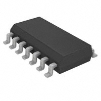
14-Lead Plastic SOIC θJC = 37˚C/W, θJA = 88˚C/W
GND
8-Lead MLP Package (5x6mm) θJC = 4˚C/W, θJA = 34˚C/W as measured on FAN1655MP Eval Board
Pin Definitions
MLP 1, 4 2, 3 PAD 5 Pin eTSSOP 1, 2, 7 3, 6 4, 5, 8 10 11 12 SOIC-14 1, 2, 7 3, 6 4, 5, 8 9 10 11 Pin Name VDD VTTFORCE VSS VTTSENSE VREFIN SHDN Pin Function Description Input power for the LDO. The VTT output voltage. IC Ground. Feedback for remote sense of the VTT voltage. Alternative input for direct control of VTTOUT and VREFOUT. Shutdown. This active low shutdown turns off both VTT and VREFOUT. This pin has an internal pull-down, and must be externally driven high for the IC to be on. Signal Ground. Buffered Voltage Reference Output. VDDQ Input. Attach this pin to the VDDQ supply to generate VTT and VREFOUT. No Internal Connection Connect PAD to Vss Ground Plane
6
7 8
13 14 15 9, 16 PAD
12 13 14
VSSQ VREFOUT VDDQ NC
PAD
Typical Application
VDDQ VDD VTTFORCE 1 2 3 4 5 6 7 8 10µF 16 15 14 FAN1655 13 12 11 10 9 1nF 470µF
10k
10µF VREFOUT SHDN VTTSENSE
GND
100µF 6V
1nF
(connect to VTTFORCE at the load) GND
Figure 1. (eTSSOP pinout shown) 2
REV. 1.1.4 3/24/04
�FAN1655
PRODUCT SPECIFICATION
Typical Performance Characteristics
Quiescent Current vs. Temperature
9
VREF Output Change vs. IREF
1.0
7.5
QUIESCENT CURRENT (mA)
VDD = VDDQ = 2.5V TA = 25˚C
0.5
4.5 3
∆ VREFOUT (mV)
6
0
-0.5
1.5 0 -60
-40
-20
0
20
40
60
80
100 120
140
-1.0 -6
-5
-4
-3
-2
-1
0
1
2
3
4
5
6
AMBIENT TEMPERATURE (˚C)
VREF LOAD CURRENT (mA)
Figure 2. Quiescent Current vs. Ambient Temperature
Figure 3. Reference Output Load Regulation
1.260
100.0 Current Pulse Duration (S)
1.255
VTT OUTPUT (V)
TA=70°C
1.250
10.0
TA=25°C
1.245
1.240 -3000
1.0
-2000 -1000 0 1000 2000 3000
1
1.5
2
2.5
3
VTT Load Current (mA)
Peak Load Current (A)
Figure 4. VTT Load Regulation
Figure 5. Maximum Non-Repetitive Output Current vs. Pulse Width (FAN1655M SO-14 Package)
REV. 1.1.4 3/24/04
3
�PRODUCT SPECIFICATION
FAN1655
Absolute Maximum Ratings
Supply Voltage VDD, VDDQ Junction Temperature, TJ Storage Temperature Lead Soldering Temperature, 10 seconds Power Dissipation, PD FAN1655M (SOIC-14) FAN1655MTF (e-TSSOP) FAN1655MP (MLP) 6V 150˚C -65 to 150˚C 300˚C 1.4W See “Power Dissipation and Derating”
Recommended Operating Conditions
Parameter Supply Voltage VDD Supply Voltage VDDQ Ambient Operating Temperature VREFIN Conditions Min. 2.3 2.2 0 1.1 1.25 Typ. 2.5 2.5 Max. 3.6 3.0 125 1.5 Units V V ˚C V
Electrical Characteristics
(VDD = VDDQ = 2.5V ± 0.2V, and TA = 25˚C using circuit in Figure 1, unless otherwise noted.) The • denotes specifications which apply over the specified operating temperature range. Parameter VTT Output Voltage Conditions IOUT = 0A, VREFIN = open VDDQ = 2.3V VDDQ = 2.5V VDDQ = 2.7V IOUT = ±2.1A, VREFIN = open VDDQ = 2.3V VDDQ = 2.5V VDDQ = 2.7V Cload = 10µF SHDN = 0V Min. • • • 1.135 1.235 1.335 1.110 1.210 1.310 Typ. 1.150 1.250 1.350 1.150 1.250 1.350 0.3 • -50 ±3.1 100 No load VREFIN = 1.150V • VREFIN = 1.250V • VREFIN = 1.350V • VDDQ = 2.3V • • SHDN = 0V • • No load, SHDN = 2.7V • SHDN = 0V • SHDN = 0V • SHDN = 2.7V • 1.145 1.245 1.345 -5 -10 1.667 1.150 1.250 1.350 1.155 1.255 1.355 5 10 0.800 20 10 50 75 V V V mA µA V V mA µA µA µA ˚C ˚C 50 Max. 1.165 1.265 1.365 1.190 1.290 1.390 Units V V V V V V V/µS µA A KΩ
VTT Output Slew Rate VTT Leakage Current VTT Current Limit VREFIN Input Impedance VREFOUT Output Voltage
VREFOUT Output Current VREFOUT Leakage Current SHDN Logic High SHDN Logic Low IDD Supply Current VDDQ Leakage Current VDD Leakage Current SHDN Input Current Over-Temperature Shutdown Over-Temperature Hysteresis
7.5 6 3 50 155 30
4
REV. 1.1.4 3/24/04
�FAN1655
PRODUCT SPECIFICATION
Applications Information
Output Capacitor selection
The JEDEC specification for DDR termination requires that VTT stay within ±40mV of VREF, which must track VDDQ/2 within 1%. During the initial load transient, the output capacitor keeps the output within spec. To stay within the 40mV window, the “load step” due to the load transient current dropping across the output capacitor’s ESR should be 25 kept to around 25mV: where ESR < ----- is given in mΩ, and ∆I ∆I is the maximum load current. For example, to handle a 3A maximum load transient, the ESR should be no greater than 8mΩ. Furthermore, the output capacitor must be able to hold the load in spec while the regulator recovers (about 15µS). A minimum value of 470µF is recommended. These requirements can be achieved by a combination of capacitors. FAN1655 requires a minimum of 5mΩ of ESR in the output and is not stable with all-ceramic output capacitors.
Power Dissipation and Derating
The maximum output current (sink or source) for a 1.25V output is:
P D ( MAX I OUT ( MAX ) = ---------------------) 1.25 (1)
where PD(MAX) is the maximum power dissipation which is:
T J ( MAX ) – T A P D ( MAX ) = --------------------------------θ JA (2)
where TJ(MAX) is the maximum die temperature of the IC and TA is the operating ambient temperature. FAN1655 has an internal thermal limit at 150°C, which defines TJ(MAX). For the SOIC-14 package, θJA is given at 88°C/W. Using equation 2, the maximum dissipation at TA = 25°C is 1.4W, which is its rated maximum dissipation. The e-TSSOP or MLP package, however, use the PCB copper to cool the IC through the thermal pad on the package bottom. For maximum dissipation, this pad should be soldered to the PCB copper, with as much copper area as possible surrounding it to cool the package. Thermal vias should be placed as close to the thermal pad as possible to transfer heat to other layers of copper on the PCB. With large areas of PCB copper for heat sinking, a θJA of under 40°C/W can easily be achieved.
REV. 1.1.4 3/24/04
5
�PRODUCT SPECIFICATION
FAN1655
Mechanical Dimensions
16-Lead eTSSOP
0.10 TYP
16
5.0 ± 0.1
9
-A4.00 -B16 9
6.4 4.4 ± 0.1 3.40 3.2 4.16 7.72
1
8
0.2 C B A ALL LEAD TIPS
PIN #1 IDENT.
(1.78)
1 8
1.2 MAX
ALL LEAD TIPS 0.1 C
+0.15 (0.90) –0.10
0.65 TYP
0.42 TYP
LAND PATTERN RECOMMENDATION
-C0.65 TYP
0.10±0.05 TYP (0.19–0.30)
0.10 M C B A
SEE DETAIL A (0.09–0.20)
1.7 MIN
9 16
1.5 MIN
12° TOP & BOTTOM R0.09MIN 0°–8° GAGE PLANE 0.25
8
1
BOTTOM VIEW
0.75 0.45 (1.00)
SEATING PLANE
DETAIL A NOTES: A. CONFORMS TO JEDEC REGISTRATION MO-153, VARIATION ABT, DATED 10/97. B. DIMENSIONS ARE IN MILLIMETERS. C. DIMENSIONS ARE EXCLUSIVE OF BURRS, MOLD FLASH, AND THE BAR EXTENSIONS. D. DIMENSIONS AND TOLERANCES PER ASME Y14.5M, 1994.
6
REV. 1.1.4 3/24/04
�PRODUCT SPECIFICATION
FAN1655
Mechanical Dimensions
14-Lead SOIC
NOTES: 1. This package conforms to JEDEC MS-012, variation AB, ISSUEC dated May, 1990. 2. All dimensions are in millimeters 3. Standard lead finished 200 microinches / 5.08 microns min. Lead/Tin (solder) oncopper
S8.71-8.51; 7.62 14 13 12 11 10 9 8
0.50
5.75 1.00 S6.20-5.80; S4.00-3.80
1
2
3
4 1.27
5
6
7 S0.51-0.35;
1.27 7.62 LAND PATTERN RECOMMENDATION
S0.50-0.25;X45˚ S0.25-0.10;z S1.75-1.35; S0.25-0.19;
S8˚-0˚
S1.27-0.40; SEATING PLANE
7
REV. 1.1.4 3/24/04
�PRODUCT SPECIFICATION
FAN1655
Mechanical Dimensions
5mmX6mm 8-Lead MLP
5.0 A B 4.50
6.0
3.50 4.25
6.25
0.25 2X
C
(1.00)
0.25 2X
C
TOP VIEW
1.27 TYP
0.65 TYP
LAND PATTERN RECOMMENDATION
0.10 C (0.25) 1.0 MAX 0.08 C 0.05 0.00
SIDE VIEW
4.25 A 1.75 1 2 3 4
C SEATING PLANE
PIN #1 IDENT. (OPTIONAL)
0.75 A 0.35
3.25 A 1.25
NOTES: A) B) C)
DOES NOT FULLY CONFORM TO JEDEC REGISTRATION MO-229, DATED 11/2001. DIMENSIONS ARE IN MILLIMETERS. DIMENSIONING AND TOLERANCES PER ASME Y14.5–1994.
8 1.27
7
6
5
0.28–0.40 A 0.10 M C A B
3.81 A
0.05 M C
BOTTOM VIEW
8
REV. 1.1.4 3/24/04
�PRODUCT SPECIFICATION
FAN1655
Ordering Information
Part Number FAN1655M FAN1655MX FAN1655MTF FAN1655MTFX FAN1655MPX Temperature Range 0°C to 125°C 0°C to 125°C 0°C to 125°C 0°C to 125°C 0°C to 125°C Package SOIC-14 SOIC-14 eTSSOP-16 eTSSOP-16 MLP-8 Packing Rails Tape and Reel Rails Tape and Reel Tape and Reel
DISCLAIMER FAIRCHILD SEMICONDUCTOR RESERVES THE RIGHT TO MAKE CHANGES WITHOUT FURTHER NOTICE TO ANY PRODUCTS HEREIN TO IMPROVE RELIABILITY, FUNCTION OR DESIGN. FAIRCHILD DOES NOT ASSUME ANY LIABILITY ARISING OUT OF THE APPLICATION OR USE OF ANY PRODUCT OR CIRCUIT DESCRIBED HEREIN; NEITHER DOES IT CONVEY ANY LICENSE UNDER ITS PATENT RIGHTS, NOR THE RIGHTS OF OTHERS. LIFE SUPPORT POLICY FAIRCHILD’S PRODUCTS ARE NOT AUTHORIZED FOR USE AS CRITICAL COMPONENTS IN LIFE SUPPORT DEVICES OR SYSTEMS WITHOUT THE EXPRESS WRITTEN APPROVAL OF THE PRESIDENT OF FAIRCHILD SEMICONDUCTOR CORPORATION. As used herein: 1. Life support devices or systems are devices or systems which, (a) are intended for surgical implant into the body, or (b) support or sustain life, and (c) whose failure to perform when properly used in accordance with instructions for use provided in the labeling, can be reasonably expected to result in a significant injury of the user. 2. A critical component in any component of a life support device or system whose failure to perform can be reasonably expected to cause the failure of the life support device or system, or to affect its safety or effectiveness.
www.fairchildsemi.com
3/24/04 0.0m 004 Stock#DS30004854 2004 Fairchild Semiconductor Corporation
�