FDPC1012S
PowerTrench® Power Clip
25V Asymmetric Dual N-Channel MOSFET
Features
General Description
Q1: N-Channel
This device includes two specialized N-Channel MOSFETs in a
Max rDS(on) = 7.0 mΩ at VGS = 4.5 V, ID = 12 A
dual package. The switch node has been internally connected to
Q2: N-Channel
enable easy placement and routing of synchronous buck
Max rDS(on) = 2.2 mΩ at VGS = 4.5 V, ID = 23 A
converters. The control MOSFET (Q1) and synchronous
SyncFETTM (Q2) have been designed to provide optimal power
Low inductance packaging shortens rise/fall times, resulting in
lower switching losses
efficiency.
MOSFET integration enables optimum layout for lower circuit
inductance and reduced switch node ringing
Applications
RoHS Compliant
Communications
Computing
General Purpose Point of Load
Pin 1
V+
LSG
GND
V+
GND
(HSD
GND
(LSS
SW
Pin 1
HSG
SW
SW
HSG
PAD9
V+(HSD)
V+
LSG SW
SW
SW
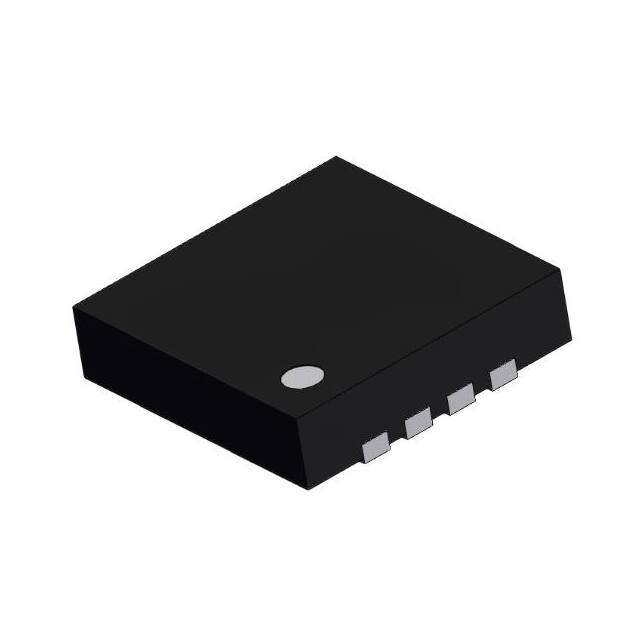
3.3 mm x 3.3 mm
LSG
SW
GND SW
PAD10
GND(LSS)
GND
GND
GND SW
SW
Top
V+
HSG
Bottom
MOSFET Maximum Ratings TA = 25 °C unless otherwise noted
Symbol
VDS
Drain to Source Voltage
Parameter
VGS
Gate to Source Voltage
Drain Current
ID
Q1
25
TJ, TSTG
V
12
12
TC = 25 °C
35
88
-Continuous
TA = 25 °C
131a
261b
40
120
(Note 4)
Single Pulse Avalanche Energy
PD
Units
V
-Continuous
-Pulsed
EAS
Q2
25
50
181
Power Dissipation for Single Operation
TA = 25 °C
(Note 3)
1.61a
2.01b
Power Dissipation for Single Operation
TA = 25 °C
0.81c
0.91d
Operating and Storage Junction Temperature Range
A
mJ
-55 to +150
W
°C
Thermal Characteristics
Thermal Resistance, Junction to Ambient
771a
RθJA
Thermal Resistance, Junction to Ambient
1c
RθJC
Thermal Resistance, Junction to Case
RθJA
151
5.0
631b
1351d
°C/W
3.5
Package Marking and Ordering Information
Device Marking
01OD/03OD
Device
FDPC1012S
©2012 Fairchild Semiconductor Corporation
FDPC1012S Rev.C1
Package
Power Clip 33
1
Reel Size
13 ”
Tape Width
12 mm
Quantity
3000 units
www.fairchildsemi.com
FDPC1012S PowerTrench® Power Clip
November 2014
�Symbol
Parameter
Test Conditions
Type
Min
25
25
Typ
Max
Units
Off Characteristics
BVDSS
Drain to Source Breakdown Voltage
ID = 250 μA, VGS = 0 V
ID = 1 mA, VGS = 0 V
Q1
Q2
ΔBVDSS
ΔTJ
Breakdown Voltage Temperature
Coefficient
ID = 250 μA, referenced to 25 °C
ID = 10 mA, referenced to 25 °C
Q1
Q2
IDSS
Zero Gate Voltage Drain Current
VDS = 20 V, VGS = 0 V
VDS = 20 V, VGS = 0 V
Q1
Q2
1
500
μA
μA
IGSS
Gate to Source Leakage Current,
Forward
VGS = 12 V/-8 V, VDS= 0 V
VGS = 12 V/-8 V, VDS= 0 V
Q1
Q2
±100
±100
nA
nA
2.2
2.2
V
V
18
22
mV/°C
On Characteristics
VGS(th)
Gate to Source Threshold Voltage
VGS = VDS, ID = 250 μA
VGS = VDS, ID = 1 mA
Q1
Q2
ΔVGS(th)
ΔTJ
Gate to Source Threshold Voltage
Temperature Coefficient
ID = 250 μA, referenced to 25 °C
ID = 10 mA, referenced to 25 °C
Q1
Q2
-4
-4
VGS = 4.5 V, ID = 12 A
VGS = 4.5 V, ID = 12 A, TJ =125 °C
Q1
5.2
7.5
7.0
10.5
VGS = 4.5 V, ID = 23 A
VGS = 4.5 V, ID = 23 A ,TJ =125 °C
Q2
1.6
2.3
2.2
3.2
VDS = 5 V, ID = 13 A
VDS = 5 V, ID = 26 A
Q1
Q2
79
200
S
Q1:
VDS = 13 V, VGS = 0 V, f = 1 MHZ
Q1
Q2
1075
3456
pF
Q1
Q2
250
885
pF
Q1
Q2
50
130
pF
rDS(on)
gFS
Drain to Source On Resistance
Forward Transconductance
0.8
1.1
1.3
1.6
mV/°C
mΩ
Dynamic Characteristics
Ciss
Input Capacitance
Coss
Output Capacitance
Crss
Reverse Transfer Capacitance
Rg
Gate Resistance
Q2:
VDS = 13 V, VGS = 0 V, f = 1 MHZ
Q1
Q2
0.1
0.1
0.4
0.5
2.0
2.0
Ω
Switching Characteristics
td(on)
Turn-On Delay Time
tr
Rise Time
td(off)
Turn-Off Delay Time
tf
Fall Time
Qg
Total Gate Charge
Qgs
Gate to Source Gate Charge
Qgd
Gate to Drain “Miller” Charge
©2012 Fairchild Semiconductor Corporation
FDPC1012S Rev.C1
Q1:
VDD = 13 V, ID = 13 A, RGEN = 6 Ω
Q2:
VDD = 13 V, ID = 26 A, RGEN = 6 Ω
VGS = 0 V to 4.5 V Q1
VDD = 13 V,
ID = 13 A
Q2
VDD = 13 V,
ID = 26 A
2
Q1
Q2
6
12
ns
Q1
Q2
2
3
ns
Q1
Q2
19
34
ns
Q1
Q2
2
3
ns
Q1
Q2
8
25
nC
Q1
Q2
2.3
7.8
nC
Q1
Q2
2.0
6.4
nC
www.fairchildsemi.com
FDPC1012S PowerTrench® Power Clip
Electrical Characteristics TJ = 25 °C unless otherwise noted
�Symbol
Parameter
Test Conditions
Type
Min
Typ
Max
Units
Q1
Q2
0.8
0.8
1.2
1.2
V
Q1
Q2
20
27
35
43
ns
Q1
Q2
6
27
12
43
nC
Drain-Source Diode Characteristics
VSD
Source to Drain Diode Forward Voltage
trr
Reverse Recovery Time
Qrr
Reverse Recovery Charge
VGS = 0 V, IS = 13 A
VGS = 0 V, IS = 26 A
(Note 2)
(Note 2)
Q1
IF = 13 A, di/dt = 100 A/μs
Q2
IF = 26 A, di/dt = 300 A/μs
Notes:
1.RθJA is determined with the device mounted on a 1 in2 pad 2 oz copper pad on a 1.5 x 1.5 in. board of FR-4 material. RθJC is guaranteed by design while RθCA is determined by
the user's board design.
b. 63 °C/W when mounted on
a 1 in2 pad of 2 oz copper
a. 77 °C/W when mounted on
a 1 in2 pad of 2 oz copper
SS
SF
DS
DF
G
SS
SF
DS
DF
G
d. 135 °C/W when mounted on a
minimum pad of 2 oz copper
c. 151 °C/W when mounted on a
minimum pad of 2 oz copper
SS
SF
DS
DF
G
SS
SF
DS
DF
G
2 Pulse Test: Pulse Width < 300 μs, Duty cycle < 2.0%.
3. Q1 :EAS of 50 mJ is based on starting TJ = 25 oC; N-ch: L = 3 mH, IAS = 5.8A, VDD = 25 V, VGS = 10 V. 100% test at L= 0.1 mH, IAS = 14.5 A.
Q2: EAS of 181 mJ is based on starting TJ = 25 oC; N-ch: L = 3 mH, IAS = 11 A, VDD = 25 V, VGS = 10 V. 100% test at L= 0.1 mH, IAS = 32.9 A.
4. Pulsed Id limited by junction temperature,td