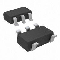
FIN1001M5

FIN1001M5

  • 厂商:

    FAIRCHILD(仙童半导体)

  • 封装:

  • 描述:

    FIN1001M5 - 3.3V LVDS 1-Bit High Speed Differential Driver - Fairchild Semiconductor

  • 详情介绍
  • 数据手册
  • 价格&库存
FIN1001M5 数据手册
FIN1001 3.3V LVDS 1-Bit High Speed Differential Driver December 2001 Revised January 2002 FIN1001 3.3V LVDS 1-Bit High Speed Differential Driver General Description This single driver is designed for high speed interconnects utilizing Low Voltage Differential Signaling (LVDS) technology. The driver translates LVTTL signal levels to LVDS levels with a typical differential output swing of 350 mV which provides low EMI at ultra low power dissipation even at high frequencies. This device is ideal for high speed transfer of clock or data. The FIN1001 can be paired with its companion receiver, the FIN1002, or with any other LVDS receiver. Features I Greater than 600Mbs data rate I 3.3V power supply operation I 0.5ns maximum differential pulse skew I 1.5ns maximum propagation delay I Low power dissipation I Power-Off protection I Meets or exceeds the TIA/EIA-644 LVDS standard I Flow-through pinout simplifies PCB layout I 5-Lead SOT23 package saves space Ordering Code: Order Number FIN1001M5 FIN1001M5X Package Number MA05B MA05B Package Description 5-Lead SOT23, JEDEC MO-178, 1.6mm [250 Units on Tape and Reel] 5-Lead SOT23, JEDEC MO-178, 1.6mm [3000 Units on Tape and Reel] Pin Descriptions Pin Name DIN DOUT+ DOUT− VCC GND NC Description LVTTL Data Input Non-inverting LVDS Driver Output Inverting LVDS Driver Output Power Supply Ground No Connect Connection Diagram Pin Assignment for SOT23 Function Table Input DIN L H H = HIGH Logic Level Outputs DOUT+ L H L = LOW Logic Level DOUT− H L (Top View) © 2002 Fairchild Semiconductor Corporation DS500721 www.fairchildsemi.com FIN1001 Absolute Maximum Ratings(Note 1) Supply Voltage (VCC) DC Input Voltage (DIN) DC Output Voltage (DOUT) Driver Short Circuit Current (IOSD) Storage Temperature Range (TSTG) Max Junction Temperature (TJ) Lead Temperature (TL) (Soldering, 10 seconds) ESD (Human Body Model) ESD (Machine Model) 260°C −0.5V to +4.6V −0.5V to +6V −0.5V to +4.6V Continuous Recommended Operating Conditions Supply Voltage (VCC) Input Voltage (VIN) Operating Temperature (TA) 3.0V to 3.6V 0 to VCC −40°C to +85°C −65°C to +150°C 150°C Note 1: The “Absolute Maximum Ratings”: are those values beyond which damage to the device may occur. The databook specifications should be met, without exception, to ensure that the system design is reliable over its power supply, temperature and output/input loading variables. Fairchild does not recommend operation of circuits outside databook specification. ≥ 7500V ≥ 500V DC Electrical Characteristics Over supply voltage and operating temperature ranges, unless otherwise specified Symbol VOD ∆VOD VOS ∆VOS IOFF IOS VIH VIL IIN II(OFF) VIK ICC CIN COUT Parameter Output Differential Voltage VOD Magnitude Change from Differential LOW-to-HIGH Offset Voltage Offset Magnitude Change from Differential LOW-to-HIGH Power-Off Output Current Short Circuit Output Current Input HIGH Voltage Input LOW Voltage Input Current Power-Off Input Current Input Clamp Voltage Power Supply Current Input Capacitance Output Capacitance VIN = 0V or VCC VCC = 0V, VIN = 0V or 3.6V IIK = −18 mA No Load, VIN = 0V or VCC RL = 100 Ω, VIN = 0V or VCC VCC = 3.3V VCC = 0V −1.5 −0.8 4.5 6.5 3.2 3.3 8 10 VCC = 0V, VOUT = 0V or 3.6V VOUT = 0V VOD = 0V 2.0 GND −5.5 ±4 RL = 100 Ω, See Figure 1 1.125 1.25 Test Conditions Min 250 Typ (Note 2) 350 450 25 1.375 25 ±20 −8 ±8 VCC 0.8 ±20 ±20 Max Units mV mV V mV µA mA V V µA µA V mA pF pF Note 2: All typical values are at TA = 25°C and with VCC = 3.3V. AC Electrical Characteristics Over supply voltage and operating temperature ranges, unless otherwise specified Symbol tPLHD tPHLD tTLHD tTHLD tSK(P) tSK(PP) Parameter Differential Propagation Delay LOW-to-HIGH Differential Propagation Delay HIGH-to-LOW Differential Output Fall Time (80% to 20%) Pulse Skew |tPLH - tPHL| Part-to-Part Skew (Note 4) RL = 100 Ω, CL = 10pF, Differential Output Rise Time (20% to 80%) See Figure 2 and Figure 3 Test Conditions Min Typ (Note 3) 0.5 0.5 0.4 0.4 0.98 0.93 0.5 0.5 0.05 1.5 1.5 1.0 1.0 0.5 1.0 Max Units ns ns ns ns ns ns Note 3: All typical values are at TA = 25°C and with VCC = 3.3V. Note 4: tSK(PP) is the magnitude of the difference in propagation delay times between any specified terminals of two devices switching in the same direction (either LOW-to-HIGH or HIGH-to-LOW) when both devices operate with the same supply voltage, same temperature, and have identical test circuits. www.fairchildsemi.com 2 FIN1001 Note A: All input pulses have frequency = 10 MHz, tR or tF = 2 ns Note B: CL includes all probe and fixture capacitances FIGURE 1. Differential Driver DC Test Circuit FIGURE 2. Differential Driver Propagation Delay and Transition Time Test Circuit FIGURE 3. AC Waveforms 3 www.fairchildsemi.com FIN1001 DC / AC Typical Performance Curves FIGURE 4. Output High Voltage vs. Power Supply Voltage FIGURE 5. Output Low Voltage vs. Power Supply Voltage FIGURE 6. Output Short Circuit Current vs. Power Supply Voltage FIGURE 7. Differential Output Voltage vs. Power Supply Voltage FIGURE 8. Differential Output Voltage vs. Load Resistor FIGURE 9. Offset Voltage vs. Power Supply Voltage www.fairchildsemi.com 4 FIN1001 DC / AC Typical Performance Curves (Continued) FIGURE 10. Power Supply Current vs. Frequency FIGURE 11. Power Supply Current vs. Power Supply Voltage FIGURE 12. Power Supply Current vs. Ambient Temperature FIGURE 13. Differential Propagation Delay vs. Power Supply FIGURE 14. Differential Propagation Delay vs. Ambient Temperature FIGURE 15. Differential Pulse Skew (tPLH - tPHL) vs. Power Supply Voltage 5 www.fairchildsemi.com FIN1001 DC / AC Typical Performance Curves (Continued) FIGURE 16. Differential Pulse Skew (tPLH - tPHL) vs. Ambient Temperature FIGURE 17. Transition Time vs. Power Supply Voltage FIGURE 18. Transition Time vs. Ambient Temperature www.fairchildsemi.com 6 FIN1001 3.3V LVDS 1-Bit High Speed Differential Driver Physical Dimensions inches (millimeters) unless otherwise noted 5-Lead SOT23, JEDEC MO-178, 1.6mm Package Number MA05B Fairchild does not assume any responsibility for use of any circuitry described, no circuit patent licenses are implied and Fairchild reserves the right at any time without notice to change said circuitry and specifications. LIFE SUPPORT POLICY FAIRCHILD’S PRODUCTS ARE NOT AUTHORIZED FOR USE AS CRITICAL COMPONENTS IN LIFE SUPPORT DEVICES OR SYSTEMS WITHOUT THE EXPRESS WRITTEN APPROVAL OF THE PRESIDENT OF FAIRCHILD SEMICONDUCTOR CORPORATION. As used herein: 1. Life support devices or systems are devices or systems which, (a) are intended for surgical implant into the body, or (b) support or sustain life, and (c) whose failure to perform when properly used in accordance with instructions for use provided in the labeling, can be reasonably expected to result in a significant injury to the user. 7 2. A critical component in any component of a life support device or system whose failure to perform can be reasonably expected to cause the failure of the life support device or system, or to affect its safety or effectiveness. www.fairchildsemi.com www.fairchildsemi.com
FIN1001M5
1. 物料型号: - FIN1001M5:5-Lead SOT23, JEDEC MO-178, 1.6mm [250 Units on Tape and Reel] - FIN1001M5X:5-Lead SOT23, JEDEC MO-178, 1.6mm [3000 Units on Tape and Reel]

2. 器件简介: - FIN1001是一款3.3V LVDS 1-Bit高速差分驱动器,利用低压差分信号技术(LVDS),将LVTTL信号电平转换为LVDS电平,具有典型的差分输出摆动为350毫伏,即使在高频下也能提供低EMI和超低功耗。该器件非常适合高速传输时钟或数据。

3. 引脚分配: - DIN:LVTTL数据输入 - DoUT+:非反相LVDS驱动器输出 - DoUT-:反相LVDS驱动器输出 - Vcc:电源 - GND:地 - NC:无连接

4. 参数特性: - 数据速率大于600Mbs - 3.3V电源操作 - 最大差分脉冲偏差为0.5纳秒 - 最大传播延迟为1.5纳秒 - 低功耗 - 掉电保护 - 满足或超过TIA/EIA-644 LVDS标准 - 直通引脚排列简化PCB布局 - 5-Lead SOT23封装节省空间

5. 功能详解: - FIN1001可以将LVTTL信号电平转换为LVDS电平,具有高速传输能力,适用于时钟或数据的高速传输。

6. 应用信息: - FIN1001可以与配套的接收器FIN1002或其他任何LVDS接收器配对使用。

7. 封装信息: - 5-Lead SOT23封装,JEDEC MO-178标准,封装体尺寸为1.6mm。
FIN1001M5 价格&库存

很抱歉,暂时无法提供与“FIN1001M5”相匹配的价格&库存,您可以联系我们找货

免费人工找货