FMB3946
Discrete Power & Signal Technologies
FMB3946
C2 E1 C1 Package: SuperSOT-6 Device Marking: .002 B2 E2 B1 Note: The " . " (dot) signifies Pin 1 Transistor 1 is NPN device, transistor 2 is PNP device.
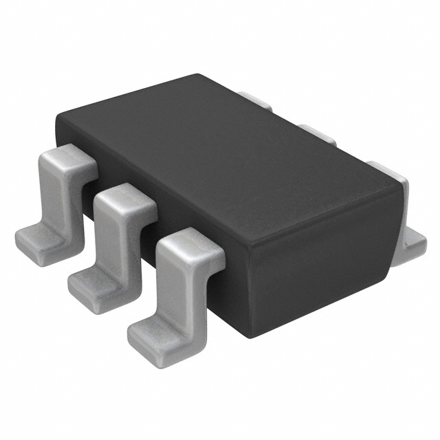
NPN & PNP Complementary Dual Transistor SuperSOT-6 Surface Mount Package
This complementary dual device was designed for use as a general purpose amplifier and switch. The useful dynamic range extends to 100mA as a switch and to 100MHz as an amplifier. Sourced from Process 23 (NPN) and Process 66 (PNP).
Absolute Maximum Ratings*
Symbol VCEO VCBO VEBO IC TJ, Tstg Parameter Collector-Emitter Voltage Collector-Base Voltage Emitter-Base Voltage Collector Current
TA
= 25°C unless otherwise noted
Value 40 40 5 200 -55 to +150
Units V V V mA °C
Operating and Storage Junction Temperature Range
*These ratings are limiting values above which the serviceability of any semiconductor device may be impaired. NOTES: 1) These ratings are based on a maximum junction temperature of 150°C. 2) These are steady state limits. The factory should be consulted on applications involving pulsed or low duty cycle operations.
Thermal Characteristics
Symbol PD RθJA
TA
= 25°C unless otherwise noted
Characteristics Total Device Dissipation Derate above 25°C Thermal Resistance, Junction to Ambient
Max 700 5.6 180
Units mW mW/°C °C/W
© 1997 Fairchild Semiconductor Corporation
Page 1 of 2
fmb3946.lwpPr23&66(Y2)
�FMB3946
(continued)
NPN & PNP Complementary Dual Transistor Electrical Characteristics
Symbol Parameter
TA
= 25°C unless otherwise noted
Test Conditions
Min
Max
Units
OFF CHARACTERISTICS BVCEO BVCBO BVEBO ICBO IEBO Collector to Emitter Voltage Collector to Base Voltage Emitter to Base Voltage Collector Cutoff Current Emitter Cutoff Current Ic = 1.0 mA Ic = 10 uA Ie = 10 uA Vcb = 30 V Veb = 4.0 V 40 40 5 50 50 V V V nA nA
ON CHARACTERISTICS hFE DC Current Gain Vce = Vce = Vce = Vce = Vce = 1V, 1V, 1V, 1V, 1V, Ic = 100uA Ic = 1.0mA Ic = 10mA Ic = 50mA Ic = 100mA 40 70 100 60 30 0.25 0.9 TYP 3 7 450 2.5 -
VCE(sat) VBE(sat)
Collector-Emitter Saturation Voltage Ic = 10mA, Ib = 1mA Base-Emitter Saturation Voltage Ic = 10mA, Ib = 1mA
V V
SMALL SIGNAL CHARACTERISTICS COB Output Capacitance CIB Input Capacitance fT NF Current Gain - Bandwidth Product Noise Figure
Vcb = 5V, f = 1MHz Veb = 0.5V, f = 1MHz Vce = 20V, Ic = 10mA, f = 100MHz Vce = 5V, Ic = 100uA, Rs = 1kohms, f = 10Hz to 15.7kHz
pF pF MHz dB
SWITCHING CHARACTERISTICS td tr ts tf Delay Time Rise Time Storage Time Fall Time Vcc = 3V, Vbe = 0.5V, Ic = 10 mA, Ib1 = 1 mA Vcc = 3V,Ic = 10 mA, Ib1 = Ib2 = 1 mA
TYP 18 20 150 40 ns ns ns ns
© 1997 Fairchild Semiconductor Corporation
Page 2 of 2
fmb3946.lwpPr23&66(Y2)
�
很抱歉,暂时无法提供与“FMB3946”相匹配的价格&库存,您可以联系我们找货
免费人工找货