FODB100, FODB101, FODB102 Single Channel Microcoupler™
July 2006
FODB100, FODB101, FODB102 Single Channel Microcoupler™
Features
■ Low profile package ■ ■ ■ ■ ■ ■ ■ ■ ■ ■
tm
Description
The FODB100, FODB101 and FODB102 single channel MICROCOUPLERS™ are all Pb-free, low profile miniature surface mount optocouplers in a Ball Grid Array (BGA) package. Each consists of an aluminum gallium arsenide (AlGaAs) infrared emitting diode driving a silicon phototransistor.
(1.20mm maximum mounted height) Land pattern allows for optimum board space savings High Current Transfer Ratio (CTR) at low IF Minimum isolation distance of 0.45mm High steady state isolation voltage of 2500Vrms Data rates up to 120Kbit/s (NRZ) Minimum creepage distance of 2mm Wide operating temperature range of -40°C to +125°C Available in tape and reel quantities of 3000 units Applicable to Pb-free Infrared Ray reflow (260°C max) UL and VDE approved
Schematic
ANODE 1
4 COLLECTOR
Applications
■ Primarily suited for DC-DC converters ■ For ground loop isolation, signal to noise isolation
CATHODE 2 3 EMITTER
Communications – chargers, adapters Consumer – appliances, set top boxes Industrial – power supplies, motor control
Package Dimensions
3.50 ± 0.10 2.50 1 2 4 3 B A 0.65 MAX
2.50 BALL #1 INDICATOR
3.50 ± 0.10
(Ø2.30)
4 BOTTOM VIEW
3
0.98 MAX Ø 0.80 MIN 0.10 C B A
1 TOP VIEW
2 0.35 MAX 0.25 MIN
1.20 MAX
0.85 MAX 0.68 MIN SEATING PLANE
NOTES: UNLESS OTHERWISE SPECIFIED A) ALL DIMENSIONS ARE IN MILLIMETERS. B) NO JEDEC REGISTRATION REFERENCE AS OF NOVEMBER 2002.
C
0.10 C
©2004 Fairchild Semiconductor Corporation
1
www.fairchildsemi.com
FODB100, FODB101, FODB102 Rev. 1.0.0
�FODB100, FODB101, FODB102 Single Channel Microcoupler™
Absolute Maximum Ratings (TA = 25°C Unless otherwise specified)
Symbol
TOTAL PACKAGE TSTG TOPR Tj EMITTER IF (avg) VR PD DETECTOR Continuous Collector Current PD VCEO VECO Power Dissipation Derate linearly (above 25°C) Collector-Emitter Voltage Emitter-Collector Voltage 50 150 1.42 75 7 mA mW mW/°C V V Continuous Forward Current Reverse Input Voltage Power Dissipation Derate linearly (above 25°C) 30 6 40 0.39 mA V mW mW/°C Storage Temperature Operating Temperature Junction Temperature -55 to +150 -40 to +125 130 °C °C °C
Parameter
Value
Units
2 FODB100, FODB101, FODB102 Rev. 1.0.0
www.fairchildsemi.com
�FODB100, FODB101, FODB102 Single Channel Microcoupler™
Electrical Characteristics (TA = 25°C Unless otherwise specified)
Individual Component Characteristics Symbol
EMITTER VF IR DETECTOR BVCEO BVECO ICEO CCE Breakdown Voltage Collector to Emitter Emitter to Collector Collector Dark Capacitance Current(1) IC = 100µA, IF = 0 IE = 100µA, IF = 0 VCE = 75V, IF = 0 VCE = 0V, f = 1MHz 8 75 7 100 V V nA pF Forward Voltage Reverse Current IF = 2mA VR = 6V 1.0 1.5 10 V µA
Parameter
Test Conditions
Min.
Typ.
Max.
Unit
Transfer Characteristics Symbol
CTR
Characteristic
Current Transfer Ratio(2)
Test Conditions
IF = 1mA, VCE = 5V
Min.
100 100 75
Typ.
Max.
Unit
% %
CTRCE(SAT) Saturated Current Transfer IF = 1.6mA, VCE = 0.4V Ratio (Collector to Emitter) IF = 1.0mA, VCE = 0.4V VCE (SAT) Saturation Voltage IF = 3.0mA, IC = 1.8mA IF = 1.6mA, IC = 1.6mA tr tf TPHL Rise Time (Non-Saturated) IC = 2mA, VCE = 5 V, RL = 1kΩ Fall Time (Non-Saturated) Propagation Delay High to Low Propagation Delay Low to High IC = 2mA, VCE = 5 V, RL = 1kΩ IF = 1.6mA, VCC = 5.0 V, RL = 750Ω IF = 1.6mA, VCC = 5.0 V, RL = 4.7kΩ IF = 1.6mA, VCC = 5.0 V, RL = 750Ω IF = 1.6mA, VCC = 5.0 V, RL = 4.7kΩ
0.4 1 5 3
V
µs
µs 12 5 19 µs
TPLH
Isolation Characteristics Symbol
VISO RISO CISO
Characteristic
Test Conditions
Min.
2500 1012
Typ.
Max.
Unit
V(rms) Ω
Steady State Isolation Voltage(3) RH ≤ 50%, TA = 25°C, t = 1 sec Resistance (input to output)(3) Capacitance (input to output)(3) VI-O = 500VDC f = 1MHz
0.3
0.5
pF
Notes: 1. The white dome area is sensitive to high intensity ambient light or any light source in the 500nm to 1200nm wavelength range. If such a light source is present, the part should be covered or protected. If the white dome is exposed to such a light source, the output leakage parameter of the phototransistor will increase. 2. CTR bin (FODB100 only) FODB101: 100% – 200% FODB102: 150% – 300% 3. Pin 1 and Pin 2 are shorted as input and Pin 3 and Pin 4 are shorted as output.
3 FODB100, FODB101, FODB102 Rev. 1.0.0
www.fairchildsemi.com
�FODB100, FODB101, FODB102 Single Channel Microcoupler™
Typical Performance Characteristics
Fig. 1 Normalized CTR vs. Temperature (VCE = 2V) Normalized CTR @ 25°C
IF = 2mA @ VCE = 2V
Fig. 2 Normalized CTR vs. Temperature (VCE = 5V) Normalized CTR @ 25°C 1.2
IF = 2mA @ VCE = 5V
1.2 1 0.8 0.6 0.4 0.2 0 25 40 60 80 100 120 140
IF = 500µA @ VCE = 2V IF = 1mA @ VCE = 2V
1 0.8 0.6 0.4 0.2 0 25 40
IF = 500µA @ VCE = 5V
IF = 1mA @ VCE = 5V
Temperature (°C)
100 60 80 Temperature (°C)
120
140
Fig. 3 Current Transfer Ratio vs. Collector to Emitter Voltage 500 400 CTR (%) 300 200 100 0 0 2 4 VCE (V) 6 8 10
2mA 1mA
Fig. 4 Current Transfer Ratio vs. Collector Saturation Voltage 350 300 250 CTR (%) 200 150 100 50 0 0 0.2 0.4 0.6 0.8 1.0 Collector Saturation Voltage (V)
2mA 1mA 500µA
500µA
Fig. 5 Baud Rate vs. Load Resistor 200 Baud Rate – Kbit/s 150 100 Vcc = 12V 50 Vcc = 5V 0 200 400 600 800 1000 1200 1400 RL - Load Resistor - Ohms 1600 IF = 1.47 mA Ta = 23C, PRSG = (28-1) BER < 10-6
4 FODB100, FODB101, FODB102 Rev. 1.0.0
www.fairchildsemi.com
�FODB100, FODB101, FODB102 Single Channel Microcoupler™
Tape and Reel Specifications
Embossed Carrier Tape Configuration
P0 T E1 D0
F K0 Wc B0 E2 W
Tc A0 P1 D1
User Direction of Feed
D imensions are in millimeter
Pkg type Optocoupler (12mm) A0 3.80 ±0.10 B0 3.80 ±0.10 W 12.0 +0.3/ –0.1 D0 1.50 +0.25/ –0.00 D1 1.50 +0.25/ –0.00 E1 1.75 ±0.10 E2 10.25 min F 5.50 ±0.05 P1 8.0 ±0.1 P0 4.0 ±0.1 K0 1.40 ±0.10 T 0.279 ±0.02 Wc 9.2 ±0.3 Tc 0.06 ±0.02
Notes: A0, B0, and K0 dimensions are determined with respect to the EIA/Jedec RS-481 rotational and lateral movement requirements (see sketches A, B, and C).
20 deg maximum Typical component cavity center line
0.5mm maximum
B0 20 deg maximum component rotation
0.5mm maximum
Sketch A (Side or Front Sectional View)
Typical component center line A0 Sketch B (Top View)
Sketch C (Top View)
Component Rotation
Component lateral movement
Component Rotation
Optocoupler Reel Configuration
W1 Measured at Hub
B Min Dim C
Dim D min Dim A max Dim N
DETAIL AA
See detail AA W3
13" Diameter Reel
W2 max Measured at Hub
Dimension are in inches and millimeters
Tape Size 12mm Reel Option 13" Dia Dim A 13.00 330 Dim B 0.059 1.5 Dim C 512 +0.020/–0.008 13 +0.5/–0.2 Dim D 0.795 20.2 Dim N 7.00 178 Dim W1 0.488 +0.078/–0.000 12.4 +2/–0 Dim W2 0.724 18.4 Dim W3 (LSL–USL) 0.469 – 0.606 11.9 – 15.4
5 FODB100, FODB101, FODB102 Rev. 1.0.0
www.fairchildsemi.com
�FODB100, FODB101, FODB102 Single Channel Microcoupler™
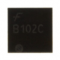
Marking Information
4
1 3 4
3
5
Definitions
1 2 6 3 4 5 6 7 Fairchild logo Device number (FODB100) One digit year code e.g. “E” for 2004 6-week date code character Die Run Code Assembly package code VDE 0884 approved (Optional)
X Y TT
B100 C V
1
2 7
2
Ball #1 Indicator
Note: The device number prefix of “FOD” will be ommitted in the part number
Recommended Footprint Drawing for PCB Layout
Ø0.65 4 3
2.50
1
2.50
2
Note: 1. All dimensions in millimeters (mm) 2. It is recommended to use 6 mils of stencil thickness on PCB
6 FODB100, FODB101, FODB102 Rev. 1.0.0
www.fairchildsemi.com
�FODB100, FODB101, FODB102 Single Channel Microcoupler™
Recommended Infrared Reflow Soldering Profile
Entrance 270.00 236.25 202.50 Zone 1 Zone 2 Zone 3 Zone 4 Zone 5 Cooling
Temperature (°C)
168.75 135.00 101.25 67.50 33.75 0.00 0.66 1.31 1.97 2.63 3.28 3.94 4.60 5.26 5.91 6.57 7.23 7.88
Time (min.)
Reflow Profile for Pb Free Convection Reflow Average ramp-up rate (183°C to peak) Preheat Temperature 125(±25)°C to 200°C Temperature maintained above 220°C Time within 5°C of actual peak temperature Peak temperature range Ramp down rate Time 25°C to peak temperature 3°C/sec max 60-180°C 60-150 sec 20-40 sec 260 ±5°C 6°C/sec max 8min max
Note: Surface Mount Adhesives (SMA) isn’t recommended to be used on the dome area (white dome).
7 FODB100, FODB101, FODB102 Rev. 1.0.0
www.fairchildsemi.com
�FODB100, FODB101, FODB102 Single Channel Microcoupler™
TRADEMARKS
The following are registered and unregistered trademarks Fairchild Semiconductor owns or is authorized to use and is not intended to be an exhaustive list of all such trademarks. ACEx™ ActiveArray™ Bottomless™ Build it Now™ CoolFET™ CROSSVOLT™ DOME™ EcoSPARK™ E2CMOS™ EnSigna™ FACT™ FAST® FASTr™ FPS™ FRFET™ FACT Quiet Series™ GlobalOptoisolator™ GTO™ HiSeC™ I2C™ i-Lo™ ImpliedDisconnect™ IntelliMAX™ ISOPLANAR™ LittleFET™ MICROCOUPLER™ MicroFET™ MicroPak™ MICROWIRE™ MSX™ MSXPro™ Across the board. Around the world.™ The Power Franchise® Programmable Active Droop™ OCX™ OCXPro™ OPTOLOGIC® OPTOPLANAR™ PACMAN™ POP™ Power247™ PowerEdge™ PowerSaver™ PowerTrench® QFET® QS™ QT Optoelectronics™ Quiet Series™ RapidConfigure™ RapidConnect™ µSerDes™ ScalarPump™ SILENT SWITCHER® SMART START™ SPM™ Stealth™ SuperFET™ SuperSOT™-3 SuperSOT™-6 SuperSOT™-8 SyncFET™ TCM™ TinyBoost™ TinyBuck™ TinyPWM™ TinyPower™ TinyLogic® TINYOPTO™ TruTranslation™ UHC™ UniFET™ UltraFET® VCX™ Wire™
DISCLAIMER
FAIRCHILD SEMICONDUCTOR RESERVES THE RIGHT TO MAKE CHANGES WITHOUT FURTHER NOTICE TO ANY PRODUCTS HEREIN TO IMPROVE RELIABILITY, FUNCTION, OR DESIGN. FAIRCHILD DOES NOT ASSUME ANY LIABILITY ARISING OUT OF THE APPLICATION OR USE OF ANY PRODUCT OR CIRCUIT DESCRIBED HEREIN; NEITHER DOES IT CONVEY ANY LICENSE UNDER ITS PATENT RIGHTS, NOR THE RIGHTS OF OTHERS. THESE SPECIFICATIONS DO NOT EXPAND THE TERMS OF FAIRCHILD’S WORLDWIDE TERMS AND CONDITIONS, SPECIFICALLY THE WARRANTY THEREIN, WHICH COVERS THESE PRODUCTS.
LIFE SUPPORT POLICY
FAIRCHILD’S PRODUCTS ARE NOT AUTHORIZED FOR USE AS CRITICAL COMPONENTS IN LIFE SUPPORT DEVICES OR SYSTEMS WITHOUT THE EXPRESS WRITTEN APPROVAL OF FAIRCHILD SEMICONDUCTOR CORPORATION. As used herein: 1. Life support devices or systems are devices or systems which, (a) are intended for surgical implant into the body, or (b) support or sustain life, or (c) whose failure to perform when properly used in accordance with instructions for use provided in the labeling, can be reasonably expected to result in significant injury to the user. 2. A critical component is any component of a life support device or system whose failure to perform can be reasonably expected to cause the failure of the life support device or system, or to affect its safety or effectiveness.
PRODUCT STATUS DEFINITIONS Definition of Terms
Datasheet Identification Advance Information Product Status Formative or In Design Definition This datasheet contains the design specifications for product development. Specifications may change in any manner without notice. This datasheet contains preliminary data, and supplementary data will be published at a later date. Fairchild Semiconductor reserves the right to make changes at any time without notice to improve design. This datasheet contains final specifications. Fairchild Semiconductor reserves the right to make changes at any time without notice to improve design. This datasheet contains specifications on a product that has been discontinued by Fairchild semiconductor. The datasheet is printed for reference information only.
Rev. I20
Preliminary
First Production
No Identification Needed
Full Production
Obsolete
Not In Production
8 FODB100, FODB101, FODB102 Rev. 1.0.0
www.fairchildsemi.com
�