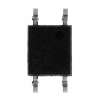
FODM121 Series, FODM124, FODM2701 Series, FODM2705 4-Pin Full Pitch Mini-Flat Package Transistor Output Optocouplers
February 2007
FODM121 Series, FODM124, FODM2701 Series, FODM2705 4-Pin Full Pitch Mini-Flat Package Transistor Output Optocouplers
Features
■ >5mm creepage/clearance ■ Compact 4-pin surface mount package ■
Applications
■ Digital logic inputs ■ Microprocessor inputs ■ Power supply monitor ■ Twisted pair line receiver ■ Telephone line receiver
■ ■ ■
(2.4mm maximum standoff height) Current Transfer Ratio in selected groups DC Input: FODM121: 50–600% FODM2701: 50–300% FODM121A: 100–300% FODM2701A: 150–300% FODM121B: 50–150% FODM2701B: 80–160% FODM121C: 100–200% FODM124: 100% MIN FODM121D: 50–100% FODM121E: 150–300% FODM121F: 100–600% FODM121G: 200–400% AC Input: FODM2705: 50–300% Available in tape and reel quantities of 500 and 2500 Applicable to Infrared Ray reflow (260°C max, 10 seconds) C-UL, UL and VDE* certifications
Description
The FODM124, FODM121, and FODM2701 series consists of a gallium arsenide infrared emitting diode driving a phototransistor in a compact 4-pin mini-flat package. The lead pitch is 2.54 mm. The FODM2705 series consists of two gallium arsenide infrared emitting diodes connected in inverse parallel for AC operation.
*option ‘V’ required
Package Dimensions
4.40±0.20
ANODE 1
4 COLLECTOR
CATHODE 2
3 EMITTER
2.54
Equivalent Circuit FODM121, FODM124, FODM2701
3.85±0.20 2.00±0.20
5.30±0.30
ANODE 1
4 COLLECTOR
0.20±0.05 0.10±0.10
CATHODE 2
3 EMITTER
0.40±0.10
7.00
+0.2 –0.7
Equivalent Circuit FODM2705
Note: All dimensions are in millimeters.
©2006 Fairchild Semiconductor Corporation
1
www.fairchildsemi.com
FODMX Rev. 1.0.7
�FODM121 Series, FODM124, FODM2701 Series, FODM2705 4-Pin Full Pitch Mini-Flat Package Transistor Output Optocouplers
Absolute Maximum Ratings (TA = 25°C unless otherwise specified)
Symbol
TOTAL PACKAGE TSTG TOPR EMITTER IF (avg) IF (pk) VR PD DETECTOR Continuous Collector Current PD VCEO VECO Power Dissipation Derate linearly (above 25°C) Collector-Emitter Voltage Emitter-Collector Voltage FODM2701 Series, FODM2705 FODM121 Series, FODM124 80 150 2.0 40 80 7 V mA mW mW/°C V Continuous Forward Current Peak Forward Current (1µs pulse, 300 pps.) Reverse Input Voltage Power Dissipation Derate linearly (above 25°C) 50 1 6 70 0.65 mA A V mW mW/°C Storage Temperature Operating Temperature -40 to +125 -40 to +110 °C °C
Parameter
Value
Units
Electrical Characteristics (TA = 25°C)
Individual Component Characteristics Symbol Parameter
EMITTER VF Forward Voltage IF = 10mA IF = 5mA IF = ±5mA IR Reverse Current VR = 5V FODM121 Series FODM124 FODM2701 Series FODM2705 FODM2701 Series FODM121 Series FODM124 DETECTOR BVCEO Breakdown Voltage Collector to Emitter IC = 1mA, IF = 0 FODM121 Series FODM124 FODM2701 Series FODM2705 BVECO ICEO CCE Emitter to Collector Collector Dark Current Capacitance IE = 100µA, IF = 0 VCE = 40V, IF = 0 VCE = 0V, f = 1MHz All All All 10 80 40 7 – 100 V nA pF V 5 µA 1.0 1.3 1.4 V
Test Conditions
Device
Min.
Typ.*
Max.
Unit
2 FODMX Rev. 1.0.7
www.fairchildsemi.com
�FODM121 Series, FODM124, FODM2701 Series, FODM2705 4-Pin Full Pitch Mini-Flat Package Transistor Output Optocouplers
Transfer Characteristics (TA = 25°C)
Symbol
CTR
Characteristic
DC Current Transfer Ratio
Test Conditions
IF = ±5mA, VCE = 5V IF = 5mA, VCE = 5V
Device
FODM2705 FODM2701 FODM2701A FODM2701B
Min.
50 50 150 80 50 100 50 100 50 150 100 200 30 100 50 0.3
Typ.** Max.
300 300 300 160 600 300 150 200 100 300 600 400 1200 3.0 0.3 0.3 0.3 0.3 0.4 0.4 0.4 0.4 0.4 0.4 0.4 0.4 0.4 0.4 3 3
Unit
%
IF = 5mA, VCE = 5V
FODM121 FODM121A FODM121B FODM121C FODM121D FODM121E FODM121F FODM121G
IF = 1mA, VCE = 0.4V IF = 1mA, VCE = 0.5V IF = 0.5mA, VCE = 1.5V CTR Symmetry VCE (SAT) Saturation Voltage IF = ±5mA, VCE = 5V IF = ±10mA, IC = 2mA IF = 10mA, IC = 2mA
FODM121F FODM124 FODM124 FODM2705 FODM2705 FODM2701 FODM2701A FODM2701B
V
IF = 8mA, IC = 2.4mA
FODM121 FODM121A FODM121B FODM121C FODM121D FODM121E FODM121F FODM121G
IF = 1mA, IC = 0.2mA IF = 1mA, IC = 0.5mA tr tf Rise Time (Non-Saturated) IC = 2mA, VCE = 5V, RL = 100Ω Fall Time (Non-Saturated) IC = 2mA, VCE = 5V, RL = 100Ω
FODM121F FODM124 All All
µs µs
Isolation Characteristics
Characteristic
Steady State Isolation Voltage(1)
Test Conditions
1 Minute
Symbol
VISO
Device
All
Min.
3750
Typ.*
Max.
Unit
VRMS
*All typicals at TA = 25°C Note: 1. Steady state isolation voltage, VISO, is an internal device dielectric breakdown rating. For this test, pins 1 and 2 are common, and pins 3 and 4 are common.
3 FODMX Rev. 1.0.7
www.fairchildsemi.com
�FODM121 Series, FODM124, FODM2701 Series, FODM2705 4-Pin Full Pitch Mini-Flat Package Transistor Output Optocouplers
Typical Performance Curves
Fig. 1 Forward Current vs. Forward Voltage
100
Fig. 2 Collector-Emitter Saturation Voltage vs. Ambient Temperature (FODM121/2701/2705)
0.35
VCE(sat) - Collector-Emitter Saturation Voltage(V)
0.30
TA = 110oC
IF - Forward Current (mA)
70oC 25 C
o
0.25 IF = 8mA IC = 2.4mA
0C -40oC
o
0.20
10
0.15 IF = 10mA IC = 2mA
0.10
0.05
1 0.6 0.8 1.0 1.2 1.4 1.6 1.8
0.00 -40
-20
0
20
40
60
80
100
120
VF - Forward Voltage (V)
TA - Ambient Temperature (°C)
Fig. 3 Current Transfer Ratio vs. Forward Current (FODM121/2701/2705)
100
Fig. 4 Collector Current vs. Forward Current (FODM121/2701/2705)
TA = 25 oC VCE = 10V
TA = 25 C
o
CTR – Current Transfer Ratio (%)
VCE = 10V VCE = 5V
IC - Collector Current (mA)
VCE = 5V 10
100
1
10 0.1 1 10 100
0.1 0.1 1 10 100
IF - Forward Current (mA)
IF - Forward Current (mA)
Fig. 5 Collector Current vs. Ambient Temperature (FODM121/2701/2705)
100 IF = 25mA
40
Fig. 6 Collector Current vs. Collector-Emitter Voltage (FODM121/2701/2705)
TA = 25 C IF = 50mA IF = 40mA 30 IF = 30mA IF = 20mA
o
IC - Collector Current (mA)
10 IF = 5mA
IF = 10mA
1
IF = 1mA
IC - Collector Current (mA)
20 IF = 10mA
0.1
IF = 0.5mA
10
IF = 5mA
VCE = 5V 0.01 -40
0
IF = 1mA
-20
0
20
40
60
80
100
120
0
2
4
6
8
10
TA - Ambient Temperature (°C)
VCE - Collector-Emitter Voltage (V)
4 FODMX Rev. 1.0.7
www.fairchildsemi.com
�FODM121 Series, FODM124, FODM2701 Series, FODM2705 4-Pin Full Pitch Mini-Flat Package Transistor Output Optocouplers
Fig 7. Collector Dark Current vs. Ambient Temperature (FODM121/2701/2705)
10000
Fig. 8 Normalized Current Transfer Ratio vs. Ambient Temperature (FODM121/2701/2705)
160
CTR – Normalized Current Transfer Ratio (%)
ICEO - Collector Dark Current (nA)
1000
VCE = 40V
140
IF = 5mA VCE = 5V
Normalized to TA = 25 C
o
120
100
100
10
80
60
1
40
0.1 -40
20
-20 0 20 40 60 80 100 120
-40
-20
0
20
40
60
80
100
120
TA - Ambient Temperature (°C)
TA - Ambient Temperature (°C)
Fig. 9 Switching Time vs. Load Resistance (FODM121/2701/2705)
VCE(sat) - Collector-Emitter Saturation Voltage(V)
1000 VCC = 5V TA = 25 C tOFF
o
Fig. 10 Collector-Emitter Saturation Voltage vs. Ambient Temperature (FODM124)
0.35 IF = 1mA IC = 0.5mA
IF = 5mA
IF = 16mA
0.30
Switching Time (µs)
0.25
100
0.20
0.15
10
tS
0.10
0.05
tON 1 1 10 100
0.00 -40
-20
0
20
40
60
80
100
120
RL - Load Resistance (kΩ)
TA - Ambient Temperature (°C)
Fig. 11 Current Transfer Ratio vs. Forward Current (FODM124)
TA = 25°C VCE = 0.5V
Fig 12. Collector Current vs. Forward Current (FODM124)
TA = 25°C VCE = 0.5V 10
CTR – Current Transfer Ratio (%)
100
IC - Collector Current (mA)
1
0.1
10 0.1 1 10
0.01 0.1
1
10
IF - Forward Current (mA)
IF - Forward Current (mA)
5 FODMX Rev. 1.0.7
www.fairchildsemi.com
�FODM121 Series, FODM124, FODM2701 Series, FODM2705 4-Pin Full Pitch Mini-Flat Package Transistor Output Optocouplers
Fig 13. Collector Current vs. Ambient Temperature (FODM124)
VCE = 0.5V IF = 10mA
Fig. 14 Collector Current vs. Collector-Emitter Voltage (FODM124)
10 TA = 25 C IF = 10mA
o
IC - Collector Current (mA)
10
IC - Collector Current (mA)
IF = 5mA
8
6
IF = 5mA
IF = 2mA IF = 1mA 1 IF = 0.5mA
4 IF = 2mA
2
IF = 1mA IF = 0.5mA
0.1 -40
0
-20
0
20
40
60
80
100
120
0.0
0.2
0.4
0.6
0.8
1.0
TA - Ambient Temperature (°C)
VCE - Collector-Emitter Voltage (V)
Fig. 15 Collector Dark Current vs. Ambient Temperature (FODM124)
160
Fig. 16 Normalized Current Transfer Ratio vs. Ambient Temperature (FODM124)
CTR – Normalized Current Transfer Ratio (%)
IF = 1mA, VCE = 0.5V Normalized to TA = 25°C
10000
VCE = 40V
140
ICEO - Collector Dark Current (nA)
1000
120
100
100
80
10
60
1
40
0.1 -40
20
-20
0
20
40
60
80
100
120
-40
-20
0
20
40
60
80
100
120
TA - Ambient Temperature (°C)
TA - Ambient Temperature (°C)
Fig. 17 Switching Time vs. Load Resistance (FODM124)
VCC = 5V IF = 1mA 1000 TA = 25°C
Switching Time (µs)
tOFF 100 tS
10 tON
1 1 10 100
RL - Load Resistance (kΩ)
6 FODMX Rev. 1.0.7
www.fairchildsemi.com
�FODM121 Series, FODM124, FODM2701 Series, FODM2705 4-Pin Full Pitch Mini-Flat Package Transistor Output Optocouplers
Ordering Information
Option
V R1 R2 R1V R2V
Description
VDE Approved Tape and Reel (500 units) Tape and Reel (2500 units) Tape and Reel (500 units) and VDE Approved Tape and Reel (2500 units) and VDE Approved
Marking Information
1
121 V X YY R
3 4 5
2 6
Definitions
1 2 3 4 5 6 Fairchild logo Device number VDE mark (Note: Only appears on parts ordered with VDE option – See order entry table) One digit year code Two digit work week ranging from ‘01’ to ‘53’ Assembly package code
7 FODMX Rev. 1.0.7
www.fairchildsemi.com
�FODM121 Series, FODM124, FODM2701 Series, FODM2705 4-Pin Full Pitch Mini-Flat Package Transistor Output Optocouplers
K0
t
P0
P 2
D0 E
A0 W1 B0 F
W
d
P
2.54 Pitch Description Tape Width Tape Thickness Sprocket Hole Pitch Sprocket Hole Dia. Sprocket Hole Location Pocket Location Symbol W t P0 D0 E F P2 Pocket Pitch Pocket Dimension P A0 B0 K0 Pocket Hole Dia. Cover Tape Width Cover Tape Thickness Max. Component Rotation or Tilt Devices Per Reel R1 R2 Reel Diameter R1 R2 D1 W1 d
D1
Dimensions (mm) 12.00 ±0.4 0.35±0.02 4.00±0.20 1.55±0.20 1.75±0.20 5.50±0.20 2.00±0.20 8.00±0.20 4.75±0.20 7.30±0.20 2.30±0.20 1.55±0.20 9.20 0.065±0.02 20° max 500 2500 178 mm (7") 330 mm (13")
8 FODMX Rev. 1.0.7
www.fairchildsemi.com
�FODM121 Series, FODM124, FODM2701 Series, FODM2705 4-Pin Full Pitch Mini-Flat Package Transistor Output Optocouplers
Footprint Drawing for PCB Layout
0.80
1.00
6.50
2.54 Note: All dimensions are in mm.
Recommended Infrared Reflow Soldering Profile
• Peak reflow temperature: 260°C (package surface temperature) • Time of temperature higher than 245°C: 40 seconds or less • Number of reflows: 3
300 250 200 150
10 s 260°C 245°C
Temperature (°C)
40 s 100 50 0 0 50 100 150 200 250 300
Time (s)
9 FODMX Rev. 1.0.7
www.fairchildsemi.com
�FODM121 Series, FODM124, FODM2701 Series, FODM2705 4-Pin Full Pitch Mini-Flat Package Transistor Output Optocouplers
FAIRCHILD SEMICONDUCTOR TRADEMARKS
The following are registered and unregistered trademarks Fairchild Semiconductor owns or is authorized to use and is not intended to be an exhaustive list of all such trademarks. FACT Quiet Series™ GlobalOptoisolator™ GTO™ HiSeC™ I2C™ i-Lo ™ ImpliedDisconnect™ IntelliMAX™ ISOPLANAR™ LittleFET™ MICROCOUPLER™ MicroFET™ MicroPak™ MICROWIRE™ MSX™ MSXPro™ Across the board. Around the world.™ The Power Franchise® Programmable Active Droop™ ACEx™ ActiveArray™ Bottomless™ Build it Now™ CoolFET™ CROSSVOLT ™ DOME™ EcoSPARK™ E2CMOS™ EnSigna™ FACT® FAST® FASTr™ FPS™ FRFET™ DISCLAIMER
FAIRCHILD SEMICONDUCTOR RESERVES THE RIGHT TO MAKE CHANGES WITHOUT FURTHER NOTICE TO ANY PRODUCTS HEREIN TO IMPROVE RELIABILITY, FUNCTION, OR DESIGN. FAIRCHILD DOES NOT ASSUME ANY LIABILITY ARISING OUT OF THE APPLICATION OR USE OF ANY PRODUCT OR CIRCUIT DESCRIBED HEREIN; NEITHER DOES IT CONVEY ANY LICENSE UNDER ITS PATENT RIGHTS, NOR THE RIGHTS OF OTHERS. THESE SPECIFICATIONS DO NOT EXPAND THE TERMS OF FAIRCHILD’S WORLDWIDE TERMS AND CONDITIONS, SPECIFICALLY THE WARRANTY THEREIN, WHICH COVERS THESE PRODUCTS.
OCX™ OCXPro™ OPTOLOGIC® OPTOPLANAR™ PACMAN™ POP™ Power247™ PowerEdge™ PowerSaver™ PowerTrench® QFET® QS™ QT Optoelectronics™ Quiet Series™ RapidConfigure™ RapidConnect™ µSerDes™ ScalarPump™
SILENT SWITCHER® SMART START™ SPM™ Stealth™ SuperFET™ SuperSOT™-3 SuperSOT™-6 SuperSOT™-8 SyncFET™ TCM™ TinyBoost™ TinyBuck™ TinyPWM™ TinyPower™ TinyLogic® TINYOPTO™ TruTranslation™ UHC®
UniFET™ VCX™ Wire™
LIFE SUPPORT POLICY
FAIRCHILD’S PRODUCTS ARE NOT AUTHORIZED FOR USE AS CRITICAL COMPONENTS IN LIFE SUPPORT DEVICES OR SYSTEMS WITHOUT THE EXPRESS WRITTEN APPROVAL OF FAIRCHILD SEMICONDUCTOR CORPORATION. As used herein: 1. Life support devices or systems are devices or systems which, (a) are intended for surgical implant into the body, or (b) support or sustain life, or (c) whose failure to perform when properly used in accordance with instructions for use provided in the labeling, can be reasonably expected to result in significant injury to the user. 2. A critical component is any component of a life support device or system whose failure to perform can be reasonably expected to cause the failure of the life support device or system, or to affect its safety or effectiveness.
PRODUCT STATUS DEFINITIONS Definition of Terms
Datasheet Identification Advance Information Product Status Formative or In Design Definition This datasheet contains the design specifications for product development. Specifications may change in any manner without notice. This datasheet contains preliminary data, and supplementary data will be published at a later date. Fairchild Semiconductor reserves the right to make changes at any time without notice to improve design. This datasheet contains final specifications. Fairchild Semiconductor reserves the right to make changes at any time without notice to improve design. This datasheet contains specifications on a product that has been discontinued by Fairchild semiconductor. The datasheet is printed for reference information only.
Rev. I22
Preliminary
First Production
No Identification Needed
Full Production
Obsolete
Not In Production
10 FODMX Rev. 1.0.7
www.fairchildsemi.com
�