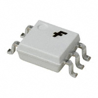
FODM452, FODM453 5-Pin Mini Flat Package High Speed Transistor Optocoupler
June 2007
FODM452, FODM453 5-Pin Mini Flat Package High Speed Transistor Optocoupler
Features
■ Compact 5-pin mini flat package ■ High speed-1 MBit/s ■ Superior CMR-15kV/µs at VCM = 1500V (FODM453) ■ Performance guaranteed over temperature (0–70°C) ■ U.L. recognized (File # E90700) ■ VDE0884 recognized (File # 136480)
tm
Description
The FODM452 and FODM453 optocouplers consist of an AlGaAs LED optically coupled to a high speed photodetector transistor. The devices are housed in a compact 5-pin mini flat package for optimum mounting density. The FODM453 features a high CMR rating for optimum common mode transient immunity.
– Ordering option V, e.g., FODM452V
Applications
■ Line receivers ■ Pulse transformer replacement ■ Output interface to CMOS-LSTTL-TTL ■ Wide bandwidth analog coupling
Package
0.050 (1.27) TYP
Schematic
ANODE 1 6 VCC
0.181 (4.60) 0.165 (4.20) SEATING PLANE
5 VO
Pin 1 0.169 (4.30) 0.153 (3.90)
CATHODE 3
4 GND
0.094 (2.40) 0.079 (2.00) 0.287 (7.30) 0.248 (6.30)
0.008 (0.2) TYP
0.020 (0.50) 0.011 (0.30)
0.008 (0.20) 0 (0.00)
Lead Coplanarity : 0.004 (0.10) MAX
Note: All dimensions are in inches (millimeters).
©2003 Fairchild Semiconductor Corporation FODM452, FODM453 Rev. 1.0.0
www.fairchildsemi.com
�FODM452, FODM453 5-Pin Mini Flat Package High Speed Transistor Optocoupler
Absolute Maximum Ratings (TA = 25°C unless otherwise noted) Stresses exceeding the absolute maximum ratings may damage the device. The device may not function or be operable above the recommended operating conditions and stressing the parts to these levels is not recommended. In addition, extended exposure to stresses above the recommended operating conditions may affect device reliability. The absolute maximum ratings are stress ratings only.
Symbol
TSTG TOPR EMITTER IF (avg) IF (pk) IF (trans) VR PD DETECTOR IO (avg) IO (pk) VCC VO PD Average Output Current Peak Output Current Supply Voltage Output Voltage Output Power Dissipation (No derating required over specified operating temp range) 8 16 -0.5 to 30 -0.5 to 20 100 mA mA V V mW DC/Average Forward Input Current Peak Forward Input Current (50% duty cycle, 1ms P.W.) Peak Transient Input Current (≤1µs P.W., 300pps) Reverse Input Voltage Input Power Dissipation (No derating required over specified operating temp range) 25 50 1.0 5 45 mA mA A V mW Storage Temperature Operating Temperature
Parameter
Value
-40 to +125 -40 to +85
Units
°C °C
©2003 Fairchild Semiconductor Corporation FODM452, FODM453 Rev. 1.0.0
www.fairchildsemi.com 2
�FODM452, FODM453 5-Pin Mini Flat Package High Speed Transistor Optocoupler
Electrical Characteristics (TA = 0 to 70°C unless otherwise specified)
Individual Component Characteristics
Symbol
EMITTER VF BVR ∆VF /∆TA DETECTOR IOH Logic High Output Current IF = 0mA, VO = VCC = 5.5V, TA =25°C IF = 0 mA, VO = VCC = 15V, TA =25°C IF = 0mA, VO = VCC = 15V ICCL ICCH Logic Low Supply Current Logic high supply current IF = 16mA, VO = Open, VCC = 15V IF = 0 mA, VO = Open, VCC = 15V, TA = 25°C IF = 0mA, VO = Open, VCC = 15V 100 0.05 .001 .001 0.5 1 50 200 1 2 µA µA µA Input Forward Voltage Input Reverse Breakdown Voltage Temperature Coefficient of Forward Voltage IF = 16mA, TA = 25°C IF = 16mA IR = 10µA IF = 16mA 5.0 -1.8 1.60 1.7 1.8 V mV/°C V
Parameter
Test Conditions
Min.
Typ.*
Max.
Unit
Transfer Characteristics
Symbol
COUPLED CTR VOL Current Transfer Ratio(1) Logic LOW Output Voltage IF = 16mA, VCC = 4.5V TA = 25°C VOL=0.4V VOL=0.5V IF = 16mA, IO = 3mA, VCC = 4.5V, TA =2 5°C IF = 16mA, IO = 2.4mA, VCC = 4.5 V 20 15 0.4 0.5 V 50 %
Parameter
Test Conditions
Min.
Typ.*
Max
Unit
Switching Characteristics (VCC = 5V)
Symbol
TPHL TPLH |CMH|
Parameter
Propagation Delay Time to Logic LOW Propagation Delay Time to Logic HIGH Common Mode Transient Immunity at Logic HIGH
Test Conditions
RL = 1.9kΩ, IF = 16mA, TA = 25°C RL = 1.9kΩ, IF = 16mA RL = 1.9kΩ, IF = 16mA
(2) (2)
Device
(Fig. 9)
Min. Typ.* Max.
0.40 0.35 0.8 1.0 0.8 1.0
Unit
µs µs µs µs KV/µs KV/µs KV/µs KV/µs MHz
(Fig. 9) (Fig. 9) FODM452 FODM453 FODM452 FODM453 5 15 5 15 15 40 15 40 3
RL = 1.9kΩ, IF = 16mA, TA = 25°C(2) (Fig. 9)
(2)
IF = 0mA, VCM = 10VP-P, RL = 1.9kΩ, TA = 25°C(3) (Fig. 10) IF = 0mA, VCM = 1500VP-P, RL = 1.9kΩ TA = 25°C(3) (Fig. 10) IF = 16mA, VCM = 10VP-P, RL = 1.9kΩ, TA = 25°C(3) (Fig. 10) IF = 16mA, VCM = 1500VP-P, RL = 1.9kΩ, TA = 25°C(3) (Fig. 10) RL = 100Ω
|CML|
Common Mode Transient Immunity at Logic LOW
BW
Bandwidth
Isolation Characteristics
Symbol
VISO CI-O
Characteristics
Withstand Insulation Test Voltage Capacitance (Input to Output) f = 1MHz
Test Conditions
RH ≤ 50%, TA = 25°C, t = 1 min.
(4) (4)
Min.
3750
Typ.*
0.2
Max.
Unit
VRMS pF
*All Typicals at TA = 25°C
©2003 Fairchild Semiconductor Corporation FODM452, FODM453 Rev. 1.0.0 www.fairchildsemi.com 3
�FODM452, FODM453 5-Pin Mini Flat Package High Speed Transistor Optocoupler
Notes: 1. Current Transfer Ratio is defined as a ratio of output collector current, IO, to the forward LED input current, IF, times 100%. 2. The 1.9kΩ load represents 1 TTL unit load of 1.6mA and 5.6kΩ pull-up resistor. 3. Common mode transient immunity in logic high level is the maximum tolerable (positive) dVcm /dt on the leading edge of the common mode pulse signal VCM, to assure that the output will remain in a logic high state (i.e., VO > 2.0V). Common mode transient immunity in logic low level is the maximum tolerable (negative) dVcm /dt on the trailing edge of the common mode pulse signal, VCM, to assure that the output will remain in a logic low state (i.e., VO < 0.8V). 4. Device is considered a two terminal device: Pins 1, and 3 are shorted together and Pins 4, 5, and 6 are shorted together.
©2003 Fairchild Semiconductor Corporation FODM452, FODM453 Rev. 1.0.0
www.fairchildsemi.com 4
�FODM452, FODM453 5-Pin Mini Flat Package High Speed Transistor Optocoupler
Typical Performance Curves
Fig. 1 Input Forward Current vs Forward Voltage
NORMALIZED CURRENT TRANSFER RATIO
100 TA = 25°C
Fig. 2 Normalized Current Transfer Ratio vs. Input Current
1.20 VO = 0.4V VCC = 5V TA = 25°C Normalized to IF = 16mA
IF – FORWARD CURRENT (mA)
10
1.15
1.10
1
1.05
0.1
1.00
0.01
0.95
0.001 1.1 1.2 1.3 1.4 1.5 1.6 1.7 1.8
0.90 1 10
VF – FORWARD CURRENT (mA)
I F – INPUT CURRENT (mA)
Fig. 3 Normalized Current Transfer Ratio vs. Ambient Temperature
NORMALIZED CURRENT TRANSFER RATIO
IF = 16mA VO = 0.4V VCC = 5V Normalized to TA = 25°C
Fig. 4 Logic High Output Current vs. Ambient Temperature
IOH – LOGIC HIGH OUTPUT CURRENT (nA)
VO = VCC = 5V IF = 0V 10
1.6 1.4 1.2 1.0 0.8 0.6 0.4 0.2 0.0 -40
1
-20
0
20
40
60
80
100
0.1 -40
-20
0
20
40
60
80
100
TA – AMBIENT TEMPERATURE
TA – TEMPERATURE (°C)
Fig. 5 DC and Pulsed Transfer Characteristics
14 TA = 25°C VCC = 5V IF = 40mA 10 35mA 30mA 8 25mA 6 20mA 15mA 4 10mA 2 5mA 10
Fig. 6 Propagation Delay vs. Load Resistance
TA = 25°C VCC = 5V IF = 16mA IF = 10mA
IO - OUTPUT CURRENT (mA)
tP – PROPAGATION DELAY (µs)
12
1
tPLH
tPHL
0 0 2 4 6 8 10 12 14 16
0.1 1 2 3 4 5 6 7 8 9 10
VO – OUTPUT VOLTAGE (V)
RL – LOAD RESISTANCE (kΩ)
©2003 Fairchild Semiconductor Corporation FODM452, FODM453 Rev. 1.0.0
www.fairchildsemi.com 5
�FODM452, FODM453 5-Pin Mini Flat Package High Speed Transistor Optocoupler
Typical Performance Curves (Continued)
Fig. 7 Propagation Delay vs. Ambient Temperature
1400 IF = 16mA VCC = 5V RL = 1.9kΩ 5 IF = 16mA VCC = 5V TA = 25°C 0
Fig. 8 Frequency Response
1200
tP – PROPAGATION DELAY (ns)
NORMALIZED RESPONSE (dB)
RL = 220Ω RL = 100Ω
1000
800
-5 RL = 470Ω
600 tPHL 400 tPLH 200
-10
RL = 1kΩ
0 -40 -20 0 20 40 60 80 100
-15 0.01
0.1
1
10
TA – AMBIENT TEMPERATURE (°C)
f – FREQUENCY (MHz)
©2003 Fairchild Semiconductor Corporation FODM452, FODM453 Rev. 1.0.0
www.fairchildsemi.com 6
�FODM452, FODM453 5-Pin Mini Flat Package High Speed Transistor Optocoupler
Pulse Generator I F tr = 5ns Z O = 50 Ω 10% D.C. I/f < 100µs
+
Noise Shield
1
6 5
VCC RL
+5 V
VO
VO 0.1 µF
I F Monitor Rm
3
4
GND
C L = 1.5 µF
IF 0
VO
5V
1.5 V
1.5 V VOL
TPHL
TPLH
Fig. 9 Switching Time Test Circuit
IF Noise Shield
+
1
A B VFF
6 5
VCC
+5 V RL VO 0.1 µF
VO
3
4
GND
-
+
VCM 10 V 10% tr VO Switch at A : IF = 0 mA VO Switch at A : IF = 16 mA
VCM
-
Pulse Gen
90%
90% 10% tf
0V
5V
VOL
Fig. 10 Common Mode Immunity Test Circuit
©2003 Fairchild Semiconductor Corporation FODM452, FODM453 Rev. 1.0.0
www.fairchildsemi.com 7
�FODM452, FODM453 5-Pin Mini Flat Package High Speed Transistor Optocoupler
Footprint Drawing for PCB Layout
0.050 0.050 0.050 (1.27) (1.27) (1.27)
0.024 (0.61)
Device ‘A’
Device ‘B’
0.190 (4.83)
0.310 (7.87)
Pin 1 0.060 (1.52)
Pin 1
0.100 (2.54) End Stacking Configuration Dimensions in inches (mm) Unutilized Solder Pad
©2003 Fairchild Semiconductor Corporation FODM452, FODM453 Rev. 1.0.0
www.fairchildsemi.com 8
�FODM452, FODM453 5-Pin Mini Flat Package High Speed Transistor Optocoupler
Ordering Information
Option
R1 R2 V R1V R2V
Order Entry Identifier (example)
FODM452R1 FODM452R2 FODM452V FODM452R1V FODM452R2V
Description
Tape and Reel (500 per reel) Tape and Reel (2500 per reel) VDE0884 VDE0884, Tape and Reel (500 per reel) VDE0884, Tape and Reel (2500 per reel)
Marking Information
1
M453 V
3 4
2 6
X YY M
5
Definitions
1 2 3 4 5 6 Fairchild logo Device number VDE mark (Note: Only appears on parts ordered with VDE option – See order entry table) One digit year code, e.g., ‘7’ Two digit work week ranging from ‘01’ to ‘53’ Assembly package code
©2003 Fairchild Semiconductor Corporation FODM452, FODM453 Rev. 1.0.0
www.fairchildsemi.com 9
�FODM452, FODM453 5-Pin Mini Flat Package High Speed Transistor Optocoupler
Carrier Tape Specifications
3.5 ± 0.2 4.0 ± 0.1 8.0 ± 0.1 2 ± 0.05 0.3 MAX Ø1.5 MIN 1.75 ± 0.10
5.5 ± 0.05 8.3 ± 0.1 12.0 ± 0.3 5.2 ± 0.2
0.1 MAX
6.4 ± 0.2 User Direction of Feed
Ø1.5 + 0.1/-0
Note: All dimensions are in millimeters.
Reflow Profile
(Heating) to 30 s Package Surface Temperature T (°C) 230°C (peak temperature) 210°C 180°C to 60 s
150 s Time (s)
90 s
80 s
• Peak reflow temperature: 230°C (package surface temperature) for 30 seconds • Time of temperature higher than 210°C: 60 seconds or less • One time soldering reflow is recommended
©2003 Fairchild Semiconductor Corporation FODM452, FODM453 Rev. 1.0.0
www.fairchildsemi.com 10
�FODM452, FODM453 5-Pin Mini Flat Package High Speed Transistor Optocoupler
TRADEMARKS The following are registered and unregistered trademarks and service marks Fairchild Semiconductor owns or is authorized to use and is not intended to be an exhaustive list of all such trademarks. ACEx Build it Now™ CorePLUS™ CROSSVOLT ™ CTL™ Current Transfer Logic™ ® EcoSPARK FACT Quiet Series™ ® FACT ® FAST FastvCore™ FPS™ ® FRFET SM Global Power Resource Green FPS™
®
Green FPS™ e-Series™ GTO™ i-Lo™ IntelliMAX™ ISOPLANAR™ MegaBuck™ MICROCOUPLER™ MicroFET™ MicroPak™ Motion-SPM™ ® OPTOLOGIC ® OPTOPLANAR PDP-SPM™ ® Power220 ® Power247
POWEREDGE Power-SPM™ ® PowerTrench Programmable Active Droop™ ® QFET QS™ QT Optoelectronics™ Quiet Series™ RapidConfigure™ SMART START™ ® SPM STEALTH™ SuperFET™ SuperSOT™-3 SuperSOT™-6
®
SuperSOT™-8 SyncFET™ ® The Power Franchise
™
TinyBoost™ TinyBuck™ ® TinyLogic TINYOPTO™ TinyPower™ TinyPWM™ TinyWire™ µSerDes™ ® UHC UniFET™ VCX™
DISCLAIMER FAIRCHILD SEMICONDUCTOR RESERVES THE RIGHT TO MAKE CHANGES WITHOUT FURTHER NOTICE TO ANY PRODUCTS HEREIN TO IMPROVE RELIABILITY, FUNCTION, OR DESIGN. FAIRCHILD DOES NOT ASSUME ANY LIABILITY ARISING OUT OF THE APPLICATION OR USE OF ANY PRODUCT OR CIRCUIT DESCRIBED HEREIN; NEITHER DOES IT CONVEY ANY LICENSE UNDER ITS PATENT RIGHTS, NOR THE RIGHTS OF OTHERS. THESE SPECIFICATIONS DO NOT EXPAND THE TERMS OF FAIRCHILD’S WORLDWIDE TERMS AND CONDITIONS, SPECIFICALLY THE WARRANTY THEREIN, WHICH COVERS THESE PRODUCTS.
LIFE SUPPORT POLICY FAIRCHILD’S PRODUCTS ARE NOT AUTHORIZED FOR USE AS CRITICAL COMPONENTS IN LIFE SUPPORT DEVICES OR SYSTEMS WITHOUT THE EXPRESS WRITTEN APPROVAL OF FAIRCHILD SEMICONDUCTOR CORPORATION. As used herein: 1. Life support devices or systems are devices or systems which, (a) are intended for surgical implant into the body or (b) support or sustain life, and (c) whose failure to perform when properly used in accordance with instructions for use provided in the labeling, can be reasonably expected to result in a significant injury of the user. 2. A critical component in any component of a life support, device, or system whose failure to perform can be reasonably expected to cause the failure of the life support device or system, or to affect its safety or effectiveness.
PRODUCT STATUS DEFINITIONS Definition of Terms Datasheet Identification Advance Information Preliminary Product Status Formative or In Design First Production Definition This datasheet contains the design specifications for product development. Specifications may change in any manner without notice. This datasheet contains preliminary data; supplementary data will be published at a later date. Fairchild Semiconductor reserves the right to make changes at any time without notice to improve design. This datasheet contains final specifications. Fairchild Semiconductor reserves the right to make changes at any time without notice to improve design. This datasheet contains specifications on a product that has been discontinued by Fairchild Semiconductor. The datasheet is printed for reference information only.
Rev. I29
No Identification Needed
Full Production
Obsolete
Not In Production
©2003 Fairchild Semiconductor Corporation FODM452, FODM453 Rev. 1.0.0
www.fairchildsemi.com 11
�