FSA2267/FSA2267A 0.35Ω Low-Voltage Dual-SPDT Analog Switch
March 2007
FSA2267 / FSA2267A 0.35Ω Low-Voltage Dual-SPDT Analog Switch
Features
■ Typical 0.35Ω On Resistance (RON) for +2.7V supply ■ FSA2267A features less than 10µA ICCT current
Description
The FSA2267 and FSA2267A are Dual Single Pole Double Throw (SPDT) analog switches. The FSA2267 operates from a single 1.65V to 3.6V supply, while the FSA2267A operates from a single 2.3V to 4.3V supply. Each features an ultra-low On Resistance of 0.35Ω at a +2.7V supply and 25°C. Both devices are fabricated with sub-micron CMOS technology to achieve fast switching speeds and designed for break-before-make operation. FSA2267A features very low quiescent current, even when the control voltage is lower than the VCC supply. This feature services the mobile handset applications very well, allowing for the direct interface with baseband processor general-purpose I/Os.
when S Input is lower than VCC
■ 0.25Ω maximum RON flatness for +2.7V supply ■ 1.6mm x 2.1mm 10-Lead MicroPak™ package ■ Broad VCC operating range ■ Low THD (0.02% typical for 32Ω load) ■ High current handling capability (350mA continuous
current under 3.3V supply)
Applications
■ Cell phone ■ PDA ■ Portable media player
Ordering Information
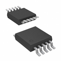
Order Number FSA2267L10X FSA2267MUX FSA2267AL10X FSA2267AMUX Top Mark FC FSA 2267 FD FSA 2267A LeadFree Yes Yes Yes Yes Package Description 10-Lead MicroPak, 1.6 x 2.1mm, JEDEC MO-255 10-Lead Molded Small Outline Package (MSOP), JEDEC MO-187, 3.0mm Wide 10-Lead MicroPak, 1.6 x 2.1mm, JEDEC MO-255 10-Lead Molded Small Outline Package (MSOP), JEDEC MO-187, 3.0mm Wide Packing Method 5000 Units on Tape and Reel 3000 Units on Tape and Reel 5000 Units on Tape and Reel 4000 Units on Tape and Reel
Lead-Free package per JEDEC J-STD-020B. MicroPak™ is a trademark of Fairchild Semiconductor Corporation.
Figure 1. Application Diagram
© 2005 Fairchild Semiconductor Corporation FSA2267 / FSA2267A Rev. 1.0.3
www.fairchildsemi.com
�FSA2267/FSA2267A 0.35Ω Low-Voltage Dual-SPDT Analog Switch
Analog Symbols
1B0 1B1 2B0 2B1 2A 2S 1A 1S
Figure 2. Analog Symbol
Connections Diagram
Vcc 1B0 1 10 9 1A
1B0
1B1 2B0 2B1 GND
1 2 3 4 5
10 9 8 7 6
Vcc 1A 1S 2S
1B1
2
8
1S
2B0
3
7
2S
2B1
4
2A
5
6
2A
Figure 3. 10-Lead MSOP
GND Figure 4. 10-Lead Micropak
Truth Table
Control Input(s) LOW Logic Level HIGH Logic Level Function B0 Connected to A B1 Connected to A
Pin Descriptions
Pin Names 1A, 2A, 1B0, 1B1, 2B0, 2B1 1S, 2S Function Data Ports Control Input
© 2005 Fairchild Semiconductor Corporation FSA2267 / FSA2267ARev. 1.0.3 2
www.fairchildsemi.com
�FSA2267/FSA2267A 0.35Ω Low-Voltage Dual-SPDT Analog Switch
Absolute Maximum Ratings
Stresses exceeding the absolute maximum ratings may damage the device. The device may not function or be operable above the recommended operating conditions and stressing the parts to these levels is not recommended. In addition, extended exposure to stresses above the recommended operating conditions may affect device reliability. The absolute maximum ratings are stress ratings only.. Symbol VCC VS VIN IIK ISW ISWPEAK TSTG TJ TL ESD Supply Voltage Switch Voltage(1) Input Voltage(1) Input Diode Current(2) Switch Current Peak Switch Current (Pulsed at 1ms duration,
很抱歉,暂时无法提供与“FSA2267AMUX”相匹配的价格&库存,您可以联系我们找货
免费人工找货