1. 物料型号:
- 型号:FST16245
- 订购代码:FST16245MTD
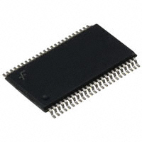
- 封装:MTD48,即48引脚薄型缩减小外型封装(TSSOP),符合JEDEC MO-153标准,宽度为6.1mm。
2. 器件简介:
- FST16245是一款16位的高速CMOS TTL兼容总线开关,具有低导通电阻和零抖动的直通模式,允许输入连接到输出而不增加传播延迟或产生额外的地弹噪声。
3. 引脚分配:
- OEn:输出使能输入(低电平有效)
- 1An, 2An, 3An, 4An:总线A
- 1Bn, 2B, 3B, 4Bn:总线B
- NC:无内部连接
4. 参数特性:
- 供电电压(Vcc):-0.5V至+7.0V
- DC开关电压(Vs):-0.5V至+7.0V
- DC输入电压(VN):-0.5V至+7.0V
- DC输入二极管电流(I):当VIN < 0V时为-50mA
- DC输出电流(Iour):128mA
- DC V/GND电流(I/GND):±100mA
- 存储温度范围(TSTG):-65°C至+150°C
5. 功能详解:
- 设备由两个8位开关组成,具有独立的输出使能输入。当OE为低电平时,开关接通,Port A连接到Port B。当OE为高电平时,开关断开,A和B端口之间存在高阻态。
- 控制输入兼容TTL电平。
6. 应用信息:
- 该器件适用于需要高速CMOS TTL兼容总线切换的应用场合。
7. 封装信息:
- 封装类型为48引脚薄型缩减小外型封装(TSSOP),符合JEDEC MO-153标准,宽度为6.1mm。