HGTG30N60C3D
D ata Sheet December 2001
63A, 600V, UFS Series N-Channel IGBT with Anti-Parallel Hyperfast Diodes
The HGTG30N60C3D is a MOS gated high voltage switching device combining the best features of MOSFETs and bipolar transistors. The device has the high input impedance of a MOSFET and the low on-state conduction loss of a bipolar transistor. The much lower on-state voltage drop varies only moderately between 25oC and 150oC. The IGBT used is the development type TA49051. The diode used in anti-parallel with the IGBT is the development type TA49053. The IGBT is ideal for many high voltage switching applications operating at moderate frequencies where low conduction losses are essential. Formerly Developmental Type TA49014.
Features
• 63A, 600V at TC = 25oC • Typical Fall Time . . . . . . . . . . . . . . . . 230ns at TJ = 150oC • Short Circuit Rating • Low Conduction Loss • Hyperfast Anti-Parallel Diode
Packaging
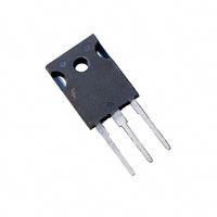
JEDEC STYLE TO-247
E C G
Ordering Information
PART NUMBER HGTG30N60C3D PACKAGE TO-247 BRAND G30N60C3D
NOTE: When ordering, use the entire part number.
Symbol
C
G
E
FAIRCHILD CORPORATION IGBT PRODUCT IS COVERED BY ONE OR MORE OF THE FOLLOWING U.S. PATENTS 4,364,073 4,598,461 4,682,195 4,803,533 4,888,627 4,417,385 4,605,948 4,684,413 4,809,045 4,890,143 4,430,792 4,620,211 4,694,313 4,809,047 4,901,127 4,443,931 4,631,564 4,717,679 4,810,665 4,904,609 4,466,176 4,639,754 4,743,952 4,823,176 4,933,740 4,516,143 4,639,762 4,783,690 4,837,606 4,963,951 4,532,534 4,641,162 4,794,432 4,860,080 4,969,027 4,587,713 4,644,637 4,801,986 4,883,767
©2001 Fairchild Semiconductor Corporation
HGTG30N60C3D Rev. B
�HGTG30N60C3D
Absolute Maximum Ratings
TC = 25oC, Unless Otherwise Specified HGTG30N60C3D 600 63 30 25 252 ±20 ±30 60A at 600V 208 1.67 -40 to 150 260 4 15 UNITS V A A A A V V W W/oC oC oC µs µs
Collector to Emitter Voltage . . . . . . . . . . . . . . . . . . . . . . . . . . . . . . . . . . . . . . . . . . . . . .BVCES Collector Current Continuous At TC = 25oC . . . . . . . . . . . . . . . . . . . . . . . . . . . . . . . . . . . . . . . . . . . . . . . . . . . . . . . . . IC25 At TC = 110oC . . . . . . . . . . . . . . . . . . . . . . . . . . . . . . . . . . . . . . . . . . . . . . . . . . . . . . . IC110 Average Diode Forward Current at 110oC . . . . . . . . . . . . . . . . . . . . . . . . . . . . . . . . . . . .I(AVG) Collector Current Pulsed (Note 1) . . . . . . . . . . . . . . . . . . . . . . . . . . . . . . . . . . . . . . . . . . . ICM Gate to Emitter Voltage Continuous. . . . . . . . . . . . . . . . . . . . . . . . . . . . . . . . . . . . . . . . . VGES Gate to Emitter Voltage Pulsed . . . . . . . . . . . . . . . . . . . . . . . . . . . . . . . . . . . . . . . . . . . .VGEM Switching Safe Operating Area at TJ = 150oC . . . . . . . . . . . . . . . . . . . . . . . . . . . . . . . . SSOA Power Dissipation Total at TC = 25oC . . . . . . . . . . . . . . . . . . . . . . . . . . . . . . . . . . . . . . . . . PD Power Dissipation Derating TC > 25oC . . . . . . . . . . . . . . . . . . . . . . . . . . . . . . . . . . . . . . . . . . Operating and Storage Junction Temperature Range . . . . . . . . . . . . . . . . . . . . . . . . TJ, TSTG Maximum Lead Temperature for Soldering . . . . . . . . . . . . . . . . . . . . . . . . . . . . . . . . . . . . . TL Short Circuit Withstand Time (Note 2) at VGE = 15V . . . . . . . . . . . . . . . . . . . . . . . . . . . . . .tSC Short Circuit Withstand Time (Note 2) at VGE = 10V . . . . . . . . . . . . . . . . . . . . . . . . . . . . . tSC
CAUTION: Stresses above those listed in “Absolute Maximum Ratings” may cause permanent damage to the device. This is a stress only rating and operation of the device at these or any other conditions above those indicated in the operational sections of this specification is not implied.
NOTES: 1. Repetitive Rating: Pulse width limited by maximum junction temperature. 2. VCE(PK) = 360V, TJ = 125oC, RG = 25Ω.
Electrical Specifications
PARAMETER
TC = 25oC, Unless Otherwise Specified SYMBOL BVCES BVECS ICES TEST CONDITIONS IC = 250µA, VGE = 0V IC = 10mA, VGE = 0V VCE = BVCES VCE = BVCES TC = 25oC TC = 150oC TC = 25oC TC = 150oC TC = 25oC MIN 600 15 3.0 VCE(PK) = 480V VCE(PK) = 600V 200 60 TYP 25 1.5 1.7 5.2 MAX 250 3.0 1.8 2.0 6.0 ±100 UNITS V V µA mA V V V nA A A
Collector to Emitter Breakdown Voltage Emitter to Collector Breakdown Voltage Collector to Emitter Leakage Current
Collector to Emitter Saturation Voltage
VCE(SAT)
IC = IC110, VGE = 15V IC = 250µA, VCE = VGE VGE = ±20V TJ = 150oC, VGE = 15V, RG = 3Ω, L = 100µH
Gate to Emitter Threshold Voltage Gate to Emitter Leakage Current Switching SOA
VGE(TH) IGES SSOA
Gate to Emitter Plateau Voltage On-State Gate Charge
VGEP QG(ON)
IC = IC110, VCE = 0.5 BVCES IC = IC110, VCE = 0.5 BVCES VGE = 15V VGE = 20V
-
8.1 162 216 40 45 320 230 1050 2500 1.75
180 250 400 275 2.2
V nC nC ns ns ns ns µJ µJ V
Current Turn-On Delay Time Current Rise Time Current Turn-Off Delay Time Current Fall Time Turn-On Energy Turn-Off Energy (Note 3) Diode Forward Voltage
td(ON)I trI td(OFF)I tfI EON EOFF VEC
TJ = 150oC, ICE = IC110, VCE(PK) = 0.8 BVCES, VGE = 15V, RG = 3Ω, L = 100µH
IEC = 30A
-
©2001 Fairchild Semiconductor Corporation
HGTG30N60C3D Rev. B
�HGTG30N60C3D
Electrical Specifications
PARAMETER Diode Reverse Recovery Time TC = 25oC, Unless Otherwise Specified SYMBOL trr TEST CONDITIONS IEC = 30A, dIEC/dt = 100A/µs IEC = 1.0A, dIEC/dt = 100A/µs Thermal Resistance RθJC IGBT Diode NOTE: 3. Turn-Off Energy Loss (EOFF) is defined as the integral of the instantaneous power loss starting at the trailing edge of the input pulse and ending at the point where the collector current equals zero (ICE = 0A). The HGTG30N60C3D was tested per JEDEC standard No. 24-1 Method for Measurement of Power Device Turn-Off Switching Loss. This test method produces the true total Turn-Off Energy Loss. Turn-On losses include diode losses. MIN TYP 52 42 MAX 60 50 0.6 1.3 UNITS ns ns
oC/W oC/W
Typical Performance Curves
ICE, COLLECTOR TO EMITTER CURRENT (A) PULSE DURATION = 250µs DUTY CYCLE


 工商网监
湘ICP备2023018690号
工商网监
湘ICP备2023018690号
