Advanced Power MOSFET
FEATURES
n Avalanche Rugged Technology n Rugged Gate Oxide Technology n Lower Input Capacitance n Improved Gate Charge n Extended Safe Operating Area n Lower Leakage Current : 10 μA (Max.) @ VDS = 100V n Lower RDS(ON) : 0.101Ω (Typ.)
IRL530A
BVDSS = 100 V RDS(on) = 0.12Ω ID = 14 A
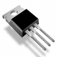
TO-220
1 2 3
1.Gate 2. Drain 3. Source
Absolute Maximum Ratings
Symbol VDSS ID IDM VGS EAS IAR EAR dv/dt PD TJ , TSTG TL Characteristic Drain-to-Source Voltage Continuous Drain Current (TC=25℃) Continuous Drain Current (TC=100℃) Drain Current-Pulsed Gate-to-Source Voltage Single Pulsed Avalanche Energy Avalanche Current Repetitive Avalanche Energy Peak Diode Recovery dv/dt Total Power Dissipation (TC=25℃) Linear Derating Factor Operating Junction and Storage Temperature Range Maximum Lead Temp. for Soldering Purposes, 1/8" from case for 5-seconds
② ① ① ③ ①
Value 100 14 9.9 49 ±20 261 14 6.2 6.5 62 0.41 - 55 to +175
Units V A A V mJ A mJ V/ns W W/℃
℃ 300
Thermal Resistance
Symbol RθJC RθCS RθJA Characteristic Junction-to-Case Case-to-Sink Junction-to-Ambient Typ. -0.5 -Max. 2.41 -62.5 ℃/W Units
Rev. B1
�IRL530A
Electrical Characteristics (TC=25℃ unless otherwise specified)
Symbol BVDSS ΔBV/ΔTJ VGS(th) IGSS IDSS RDS(on) gfs Ciss Coss Crss td(on) tr td(off) tf Qg Qgs Qgd Characteristic Drain-Source Breakdown Voltage Breakdown Voltage Temp. Coeff. Gate Threshold Voltage Gate-Source Leakage , Forward Gate-Source Leakage , Reverse Drain-to-Source Leakage Current Static Drain-Source On-State Resistance Forward Transconductance Input Capacitance Output Capacitance Reverse Transfer Capacitance Turn-On Delay Time Rise Time Turn-Off Delay Time Fall Time Total Gate Charge Gate-Source Charge Gate-Drain("Miller") Charge Min. Typ. Max. Units 100 -1.0 -----------------0.1 ------10.2 --2.0 100 -100 10 100 0.12 -μA Ω Ω V V/℃ V nA
N-CHANNEL POWER MOSFET
Test Condition VGS=0V,ID=250μA ID=250μA VGS=20V VGS=-20V VDS=100V VDS=80V,TC=150℃ VGS=5V,ID=7A VDS=40V,ID=7A
④ ④
See Fig 7
VDS=5V,ID=250μA
580 755 140 175 60 10 11 29 15 16.9 2.7 9.7 75 30 30 70 40 24 --nC ns pF
VGS=0V,VDS=25V,f =1MHz See Fig 5 VDD=50V,ID=14A, RG=6Ω See Fig 13 VDS=80V,VGS=5V, ID=14A See Fig 6 & Fig 12 ④ ⑤
④⑤
Source-Drain Diode Ratings and Characteristics
Symbol IS ISM VSD trr Qrr Characteristic Continuous Source Current Pulsed-Source Current Diode Forward Voltage Reverse Recovery Time Reverse Recovery Charge
① ④
Min. Typ. Max. Units --------109 0.41 14 49 1.5 --A V ns μC
Test Condition Integral reverse pn-diode in the MOSFET TJ=25℃,IS=14A,VGS=0V TJ=25℃,IF=14A diF/dt=100A/μs
④
Notes ; ① Repetitive Rating : Pulse Width Limited by Maximum Junction Temperature ② L=2mH, IAS=14A, VDD=25V, RG=27Ω, Starting TJ =25℃ ③ ISD≤14A, di/dt≤350A/μs, VDD≤BVDSS , Starting TJ =25℃ ④ Pulse Test : Pulse Width = 250μs, Duty Cycle ≤ 2% ⑤ Essentially Independent of Operating Temperature
�N-CHANNEL POWER MOSFET
Fig 1. Output Characteristics
12 0
VGS Top : 7.0 V 6.0 V 5.5 V 5.0 V 4.5 V 4.0 V 3.5 V Bottom : 3.0 V
IRL530A
Fig 2. Transfer Characteristics
ID , Drain Current [A]
ID , Drain Current [A]
11 0
11 0
1 5 oC 7 10 0 2 oC 5 @Nts: oe 1 V =0V . GS 2 V =4 V . DS 0 3 2 0 µs P l e T s .5 us et 4 6 8 1 0
10 0 1 -1 0 10 0
@Nts: oe 1 2 0 µs P l e T s .5 us et 2 T = 2 oC .C 5 11 0
- 5 oC 5 1 -1 0 0 2
VDS , Drain-Source Voltage [V]
VGS , Gate-Source Voltage [V]
Fig 3. On-Resistance vs. Drain Current
02 .0
Fig 4. Source-Drain Diode Forward Voltage
IDR , Reverse Drain Current [A]
RDS(on) , [ Ω ] Drain-Source On-Resistance
01 .5
V =5V GS
11 0
01 .0
V =1 V 0 GS 00 .5 @ N t : T = 2 oC oe J 5 00 .0 0 1 5 3 0 4 5 6 0
10 0 @Nts: oe 1 V =0V . GS us et 2 2 0 µs P l e T s .5 10 . 12 . 14 . 16 . 18 . 20 . 22 .
1 5 oC 7 2 oC 5 1 0
-1
04 .
06 .
08 .
ID , Drain Current [A]
VSD , Source-Drain Voltage [V]
Fig 5. Capacitance vs. Drain-Source Voltage
10 00 C =C +C (C =sotd) iss gs gd ds h r e C =C +C oss ds gd C =C rss gd 6
Fig 6. Gate Charge vs. Gate-Source Voltage
VGS , Gate-Source Voltage [V]
80 0
C iss
V =2 V 0 DS V =5 V 0 DS V =8 V 0 DS 4
Capacitance [pF]
60 0 C oss 40 0 C rss 20 0 @Nts: oe 1 V =0V . GS 2 f=1Mz . H
2
@Nts:I =1 A oe 4 D 0 0 3 6 9 1 2 1 5 1 8
00 1 0
11 0
VDS , Drain-Source Voltage [V]
QG , Total Gate Charge [nC]
�IRL530A
Fig 7. Breakdown Voltage vs. Temperature
12 . 30 .
N-CHANNEL POWER MOSFET
Fig 8. On-Resistance vs. Temperature
Drain-Source Breakdown Voltage
11 .
RDS(on) , (Normalized) Drain-Source On-Resistance
25 .
BVDSS , (Normalized)
20 .
10 .
15 .
10 . @Nts: oe 1 V =5V . GS 2 I =7A .D -0 5 -5 2 0 2 5 5 0 7 5 10 0 15 2 10 5 15 7 20 0
09 .
@Nts: oe 1 V =0V .
GS D
05 .
2 I = 2 0 µA . 5 08 . -5 7 -0 5 -5 2 0 2 5 5 0 7 5 10 0 15 2
o
10 5
15 7
20 0
00 . -5 7
TJ , Junction Temperature [ C]
TJ , Junction Temperature [oC]
Fig 9. Max. Safe Operating Area
Oeaini Ti Ae prto n hs ra i Lmtdb R s iie y
Fig 10. Max. Drain Current vs. Case Temperature
1 5
12 0
ID , Drain Current [A]
ID , Drain Current [A]
12 0
DS(on)
1 2
1 0 µs 0 1m s 11 0 D C
0
9
1m 0s
6
1 0
@Nts: oe 1 T = 2 oC . 5
C J
7 2 T = 1 5 oC . 3 Snl Ple . ige us 1 -1 0 0 1 0 11 0
3
0 2 5
5 0
7 5
10 0
15 2
10 5
15 7
VDS , Drain-Source Voltage [V]
Tc , Case Temperature [oC]
Fig 11. Thermal Response
Thermal Response
100
D=0.5 @ Notes : 1. Z J C (t)=2.41
θ
0.2 0.1 0.05
o
C/W Max.
2. Duty Factor, D=t1 /t2 3. TJ M -TC =PD M *Z
PDM t1
θJC
(t)
Z (t) ,
10- 1
0.02 0.01 single pulse
θJC
t2
10- 5
10- 4
10- 3
10- 2
10- 1
100
101
t 1 , S quare Wave Pulse Duration
[sec]
�N-CHANNEL POWER MOSFET
Fig 12. Gate Charge Test Circuit & Waveform
IRL530A
* Current Regulator ”
50KΩ 12V 200nF 300nF
Same Type as DUT
VGS Qg
10V
VDS VGS DUT
3mA
Qgs
Qgd
R1
Current Sampling (IG) Resistor
R2
Current Sampling (ID) Resistor
Charge
Fig 13. Resistive Switching Test Circuit & Waveforms
RL Vout Vin RG DUT Vin 10V
td(on) t on tr td(off) t off tf 10%
Vout VDD
( 0.5 rated VDS )
90%
Fig 14. Unclamped Inductive Switching Test Circuit & Waveforms
LL VDS
Vary tp to obtain required peak ID
BVDSS 1 EAS = ---- LL IAS2 -------------------2 BVDSS -- VDD BVDSS IAS C VDD VDD
tp
ID
RG DUT 5V
tp
ID (t) VDS (t) Time
�IRL530A
Fig 15. Peak Diode Recovery dv/dt Test Circuit & Waveforms
N-CHANNEL POWER MOSFET
DUT
+ VDS --
IS L Driver RG VGS
Same Type as DUT
VGS
VDD
• dv/dt controlled by "RG" • IS controlled by Duty Factor "D"
VGS ( Driver )
Gate Pulse Width D = -------------------------Gate Pulse Period
10V
IFM , Body Diode Forward Current
IS ( DUT ) IRM
di/dt
Body Diode Reverse Current
VDS ( DUT )
Body Diode Recovery dv/dt
Vf
VDD
Body Diode Forward Voltage Drop
�TRADEMARKS
The following are registered and unregistered trademarks Fairchild Semiconductor owns or is authorized to use and is not intended to be an exhaustive list of all such trademarks.
ACEx™ Bottomless™ CoolFET™ CROSSVOLT ™ DOME™ EcoSPARK™ E2CMOSTM EnSignaTM FACT™ FACT Quiet Series™ FAST ®
DISCLAIMER
FASTr™ FRFET™ GlobalOptoisolator™ GTO™ HiSeC™ I2C™ ISOPLANAR™ LittleFET™ MicroFET™ MicroPak™ MICROWIRE™
OPTOLOGIC ® OPTOPLANAR™ PACMAN™ POP™ Power247™ PowerTrench ® QFET™ QS™ QT Optoelectronics™ Quiet Series™ SILENT SWITCHER ®
SMART START™ SPM™ Stealth™ SuperSOT™-3 SuperSOT™-6 SuperSOT™-8 SyncFET™ TinyLogic™ TruTranslation™ UHC™ UltraFET ®
VCX™
FAIRCHILD SEMICONDUCTOR RESERVES THE RIGHT TO MAKE CHANGES WITHOUT FURTHER NOTICE TO ANY PRODUCTS HEREIN TO IMPROVE RELIABILITY, FUNCTION OR DESIGN. FAIRCHILD DOES NOT ASSUME ANY LIABILITY ARISING OUT OF THE APPLICATION OR USE OF ANY PRODUCT OR CIRCUIT DESCRIBED HEREIN; NEITHER DOES IT CONVEY ANY LICENSE UNDER ITS PATENT RIGHTS, NOR THE RIGHTS OF OTHERS.
LIFE SUPPORT POLICY FAIRCHILD’S PRODUCTS ARE NOT AUTHORIZED FOR USE AS CRITICAL COMPONENTS IN LIFE SUPPORT DEVICES OR SYSTEMS WITHOUT THE EXPRESS WRITTEN APPROVAL OF FAIRCHILD SEMICONDUCTOR CORPORATION. As used herein: 1. Life support devices or systems are devices or 2. A critical component is any component of a life systems which, (a) are intended for surgical implant into support device or system whose failure to perform can the body, or (b) support or sustain life, or (c) whose be reasonably expected to cause the failure of the life failure to perform when properly used in accordance support device or system, or to affect its safety or with instructions for use provided in the labeling, can be effectiveness. reasonably expected to result in significant injury to the user. PRODUCT STATUS DEFINITIONS Definition of Terms Datasheet Identification Advance Information Product Status Formative or In Design Definition This datasheet contains the design specifications for product development. Specifications may change in any manner without notice. This datasheet contains preliminary data, and supplementary data will be published at a later date. Fairchild Semiconductor reserves the right to make changes at any time without notice in order to improve design. This datasheet contains final specifications. Fairchild Semiconductor reserves the right to make changes at any time without notice in order to improve design.
Preliminary
First Production
No Identification Needed
Full Production
Obsolete
Not In Production
This datasheet contains specifications on a product that has been discontinued by Fairchild semiconductor. The datasheet is printed for reference information only.
Rev. H7
�


 工商网监
湘ICP备2023018690号
工商网监
湘ICP备2023018690号