KSE13003 — NPN Silicon Transistor
March 2008
KSE13003 NPN Silicon Transistor
High Voltage Switch Mode Applications
• High Voltage Capability • High Speed Switching • Suitable for Switching Regulator and Motor Control
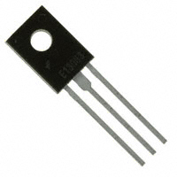
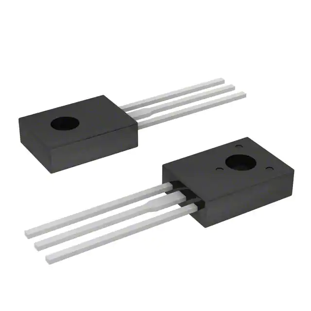
1
TO-126 2.Collector 3.Base
1. Emitter
Absolute Maximum Ratings*
Symbol
V CBO V CEO V EBO IC ICP IB PC TJ TSTG Collector-Base Voltage Collector-Emitter Voltage Emitter-Base Voltage Collector Current (DC) Collector Current (Pulse) Base Current
T C = 25°C unless otherwise noted (notes_1)
Parameter
Value
700 400 9 1.5 3 0.75 20 150 -65 ~ 150
Units
V V V A A A W °C °C
Collector Dissipation (TC = 25°C) Junction Temperature Storage Temperature Range
* These ratings are limiting values above which the serviceability of any semiconductor device may be impaired. NOTES_1: 1) These ratings are based on a maximum junction temperature of 150°C. 2) These are steady state limits. The factory should be consulted on applications involving pulsed or low duty cycle operations.
hFE Classification
Classification
hFE*
* Test on VCE = 2V, IC = 0.5A.
H1
9 ~ 16
H2
14~ 21
H3
19 ~ 26
© 2007 Fairchild Semiconductor Corporation KSE13003 Rev. 1.0.0 1
www.fairchildsemi.com
�KSE13003 — NPN Silicon Transistor
Electrical Characteristics
Symbol
BVCEO IEBO hFE VCE(sat)
TC = 25°C unless otherwise noted
Parameter
Collector-Emitter Breakdown Voltage Emitter Cut-off Current *DC Current Gain *Collector Emitter Saturation Voltage
Conditions
IC = 5mA, IB = 0 VEB = 9V, IC = 0 VCE = 2V, IC = 0.5A VCE = 2V, IC =1A IC = 0.5A, IB = 0.1A IC = 1A, IB = 0.25A IC = 1.5A, IB = 0.5A IC = 0.5A, IB = 0.1A IC = 1A, IB = 0.25A VCB = 10V , f = 0.1MHz VCE = 10V, IC = 0.1A VCC =125V, IC = 1A IB1 = 0.2A, IB2 = - 0.2A RL = 125W
Min.
400
Typ.
Max
10
Units
V mA
8 5
40 0.5 1 3 1 1.2 21 V V V V V pF MHz 1.1 4.0 0.7 ms ms ms
VBE(sat) Cob fT tON tSTG tF
*Base Emitter Saturation Voltage Output Capacitance Current Gain Bandwidth Product Turn On Time Storage Time Fall Time
4
* Pulse Test: Pulse Width=5ms, Duty Cycle£10%
Package Marking and Ordering Information
Device Item (notes_2)
KSE13003H1ASTU KSE13003H2ASTU KSE13003H3ASTU
Notes_2 : 1) The Affix “-H1/-H2/-H3” means the hFE classification. 2) The Sufix “-STU” means the TO126 short lead package and the Tube packing method, which can be on fairchildsemi website at http://www.fairchildsemi.com
Device Marking
1 E13003 2 E13003 3 E13003
Package
TO-126 TO-126 TO-126
Packing Method
TUBE TUBE TUBE
Remarks
© 2007 Fairchild Semiconductor Corporation KSE13003 Rev. 1.0.0 2
www.fairchildsemi.com
�KSE13003 — NPN Silicon Transistor
Typical Performance Characteristics
2.0
100
IC[A], COLLECTOR CURRENT
1.6
hFE, DC CURRENT GAIN
IB = 500mA IB = 450mA IB = 400mA
VCE = 2V
1.2
IB = 350mA IB = 300mA IB = 250mA IB = 200mA IB = 150mA IB = 100mA IB = 50mA
10
0.8
1
0.4
IB = 0mA
0.0 0 1 2 3 4 5
0.1 0.01
0.1
1
10
VCE[V], COLLECTOR-EMITTER VOLTAGE
IC[A], COLLECTOR CURRENT
Figure 1. Static Characteristic
Figure 2. DC current Gain
VBE(sat), VCE(sat)[V], SATURATION VOLTAGE
10
10
IC = 4 IB
tSTG, tF[ms], TIME
1
VBE(sat)
tSTG
1
tF
0.1
0.1
VCE(sat)
0.01 0.01
0.1
1
10
0.01 0.1
1
IC[A], COLLECTOR CURRENT
IC[A], COLLECTOR CURRENT
Figure 3. Base-Emitter Saturation Voltage Collector-Emitter Saturation Voltage
Figure 4. Switching Time
10
30
ICMAX. (pulse)
ms 10
25
s 1m
IC[A], COLLECTOR CURRENT
PC[W], POWER DISSIPATION
IC MAX. (DC)
1
s 5m
s 0m 10
20
15
0.1
10
5
0.01
0
1
10
100
1000
0
25
50
o
75
100
125
150
175
VCE[V], COLLECTOR-EMITTER VOLTAGE
TC[ C], CASE TEMPERATURE
Figure 5. Safe Operating Area
© 2007 Fairchild Semiconductor Corporation KSE13003 Rev. 1.0.0 3
Figure 6. Power Derating
www.fairchildsemi.com
�KSE13003 KSE13003 NPN Silicon Transistor
© 2 007 Fairchild Semiconductor Corporation KSE13003 Rev. 1.0.0 4
www.fairchildsemi.com
�
很抱歉,暂时无法提供与“KSE13003H2ASTU”相匹配的价格&库存,您可以联系我们找货
免费人工找货- 国内价格
- 20+8.339
- 200+7.801
- 500+7.263
- 1000+6.725
- 3000+6.456
- 6000+6.0794


 工商网监
湘ICP备2023018690号
工商网监
湘ICP备2023018690号
