MM74C901 • MM74C902 Hex Inverting TTL Buffer • Hex Non-Inverting TTL Buffer
October 1987 Revised January 1999
MM74C901 • MM74C902 Hex Inverting TTL Buffer • Hex Non-Inverting TTL Buffer
General Description
The MM74C901 and MM74C902 hex buffers employ complementary MOS to achieve wide supply operating range, low power consumption, and high noise immunity. These buffers provide direct interface from PMOS into CMOS or TTL and direct interface from CMOS to TTL or CMOS operating at a reduced VCC supply.
Features
s Wide supply voltage range: s Guaranteed noise margin: s High noise immunity: 3.0V to 15V 1.0V 0.45 VCC (typ.)
s TTL compatibility: Fan out of 2 driving standard TTL
Ordering Code:
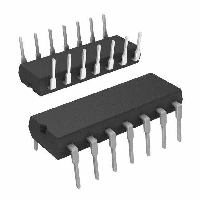
Order Number MM74C901M MM74C901N MM74C902M MM74C902N Package Number M14A N14A M14A N14A Package Description 14-Lead Small Outline Integrated Circuit (SOIC), JEDEC MS-120, 0.150” Narrow 14-Lead Plastic Dual-In-Line Package (PDIP), JEDEC MS-011, 0.300” Wide 14-Lead Small Outline Integrated Circuit (SOIC), JEDEC MS-120, 0.150” Narrow 14-Lead Plastic Dual-In-Line Package (PDIP), JEDEC MS-011, 0.300” Wide
Devices also available in Tape and Reel. Specify by appending the suffix letter “X” to the ordering code.
Connection Diagrams
Pin Assignments for DIP and SOIC MM74C901 MM74C902
Top View
Top View
Logic Diagrams
MM74C901 CMOS to TTL Inverting Buffer MM74C902 CMOS to TTL Buffer
© 1999 Fairchild Semiconductor Corporation
DS005909.prf
www.fairchildsemi.com
�MM74C901 • MM74C902
Absolute Maximum Ratings(Note 1)
Voltage at Any Pin Voltage at Any Input Pin MM74C901 MM74C902 Storage Temperature Range (TS) Power Dissipation (PD) Dual-In-Line Small Outline Operating Temperature Range (TA) MM74C901, MM74C902, −40°C to +85°C 700 mW 500 mW −0.3V to +15V −0.3V to +15V −65°C to +150°C −0.3V to VCC + 0.3V
Operating VCC Range Absolute Maximum VCC Lead Temperature (TL) (Soldering, 10 seconds)
3.0V to 15V 18V 260°C
Note 1: “Absolute Maximum Ratings” are those values beyond which the safety of the device cannot be guaranteed. Except for “Operating Temperature Range” they are not meant to imply that the devices should be operated at these limits. The table of “Electrical Characteristics” provides conditions for actual device operation.
DC Electrical Characteristics
Min/Max limits apply across temperature range unless otherwise noted Symbol CMOS TO CMOS V IN(1) V IN(0) V OUT(1) V OUT(0) I IN(1) I IN(0) I CC V IN(1) V IN(0) V IN(1) Logical “1” Input Voltage Logical “0” Input Voltage Logical “1” Output Voltage Logical “0” Output Voltage Logical “1” Input Current Logical “0” Input Current Supply Current Logical “1” Input Voltage Logical “0” Input Voltage Logical “1” Input Voltage MM74C901 MM74C902 V IN(0) Logical “0” Input Voltage MM74C901 MM74C902 V OUT(1) V OUT(0) Logical “1” Output Voltage Logical “0” Output Voltage MM74C901 MM74C902 (MM74C901) I SOURCE I SOURCE I SINK I SINK Output Source Current (P-Channel) Output Source Current (P-Channel) Output Sink Current (N-Channel) Output Sink Current (N-Channel) (MM74C902) V CC = 5.0V, VOUT = 0V T A = 25°C, VIN = 0V V CC = 10V, VOUT = 0V T A = 25°C, VIN = 0V V CC = 5.0V, VOUT = VCC T A = 25°C, VIN = VCC V CC = 5.0V, VOUT = 0.4V T A = 25°C, VIN = VCC 3.8 mA 9.0 mA −20 mA −5.0 mA V CC = 4.75V, IO = 2.6 mA V CC = 4.75V, IO = 3.2 mA 0.4 0.4 V V V CC = 4.75V V CC = 4.75V V CC = 4.75V, IO = −800 µA 2.4 1.0 1.5 V V V V CC = 4.75V V CC = 4.75V 4.25 V CC − 1.5 V V V CC = 5.0V V CC = 10V V CC = 5.0V V CC = 10V V CC = 5.0V, IO = −10 µA V CC = 10V, IO = −10 µA V CC = 5.0V V CC = 10V V CC = 15V, VIN = 15V V CC = 15V, VIN = 0V V CC = 15V V CC = 4.75V V CC = 4.75V V CC − 1.5 0.8 −1.0 0.005 −0.005 0.05 15 4.5 9.0 0.5 1.0 1.0 3.5 8.0 1.5 2.0 V V V V V V V V µA µA µA V V Parameter Conditions Min Typ Max Units
TTL TO CMOS
CMOS TO TTL
OUTPUT DRIVE (See Family Characteristics Data Sheet) (Short Circuit Current)
www.fairchildsemi.com
2
�MM74C901 • MM74C902
DC Electrical Characteristics
Symbol I SOURCE I SOURCE I SINK I SINK Parameter Output Source Current (P-Channel) Output Source Current (P-Channel) Output Sink Current (N-Channel) Output Sink Current (N-Channel)
(Continued)
Conditions V CC = 5.0V, VOUT = 0V T A = 25°C, VIN = VCC V CC = 10V, VOUT = 0V T A = 25°C, VIN = VCC V CC = 5.0V, VOUT = VCC T A = 25°C, VIN = 0V V CC = 5.0V, VOUT = 0.4V T A = 25°C, VIN = 0V
Min −5.0 −20 9.0 3.8
Typ
Max
Units mA mA mA mA
AC Electrical Characteristics
TA = 25°C, CL = 50 pF, unless otherwise noted Symbol MM74C901 t pd1 t pd0 C IN C PD t pd1 t pd0 C IN C PD Propagation Delay Time to a Logical “1” Propagation Delay Time to a Logical “0” Input Capacitance Power Dissipation Capacity Propagation Delay Time to a Logical “1” Propagation Delay Time to a Logical “0” Input Capacitance Power Dissipation Capacity Parameter
(Note 2)
Conditions Min Typ Max Units
V CC = 5.0V V CC = 10V V CC = 5.0V V CC = 10V Any Input (Note 3) Per Buffer (Note 4) V CC = 5.0V V CC = 10V V CC = 5.0V V CC = 10V Any Input (Note 3) Per Buffer (Note 4)
38 22 21 13 14 30 57 27 54 25 5.0 50
70 30 35 20
ns ns ns ns pF pF
MM74C902 90 40 90 40 ns ns ns ns pF pF
Note 2: AC Parameters are guaranteed by DC correlated testing. Note 3: C apacitance is guaranteed by periodic testing. Note 4: CPD determines the no load AC power consumption of any CMOS device. For complete explanation see Family Characteristics application note AN-90.
Typical Application
CMOS to TTL or CMOS at a Lower VCC
Note: V CC1 = VCC2
3
www.fairchildsemi.com
�MM74C901 • MM74C902
AC Test Circuit and Switching Time Waveforms
CMOS to CMOS
Note: Delays measured with input tr, tf = 20 ns.
Typical Performance Characteristics
Typical Propagation Delay to a Logical “0” for the MM74C901 Typical Propagation Delay to a Logical “1” for the MM74C901
Typical Propagation Delay to a Logical “0” for the MM74C902
Typical Propagation Delay to a Logical “1” for the MM74C902
www.fairchildsemi.com
4
�MM74C901 • MM74C902
Physical Dimensions inches (millimeters) unless otherwise noted
14-Lead Plastic Dual-In-Line Package (PDIP), JEDEC MS-120, 0.150” Narrow Package Number M14A
5
www.fairchildsemi.com
�MM74C901 • MM74C902 Hex Inverting TTL Buffer • Hex Non-Inverting TTL Buffer
Physical Dimensions inches (millimeters) unless otherwise noted (Continued)
14-Lead Plastic Dual-In-Line Package (PDIP), JEDEC MS-001, 0.300” Wide Package Number N14A
LIFE SUPPORT POLICY FAIRCHILD’S PRODUCTS ARE NOT AUTHORIZED FOR USE AS CRITICAL COMPONENTS IN LIFE SUPPORT DEVICES OR SYSTEMS WITHOUT THE EXPRESS WRITTEN APPROVAL OF THE PRESIDENT OF FAIRCHILD SEMICONDUCTOR CORPORATION. As used herein: 2. A critical component in any component of a life support 1. Life support devices or systems are devices or systems device or system whose failure to perform can be reawhich, (a) are intended for surgical implant into the sonably expected to cause the failure of the life support body, or (b) support or sustain life, and (c) whose failure device or system, or to affect its safety or effectiveness. to perform when properly used in accordance with instructions for use provided in the labeling, can be reasonably expected to result in a significant injury to the www.fairchildsemi.com user.
Fairchild does not assume any responsibility for use of any circuitry described, no circuit patent licenses are implied and Fairchild reserves the right at any time without notice to change said circuitry and specifications.
�