MM74C912 6-Digit BCD Display Controller/Driver
October 1987 Revised January 1999
MM74C912 6-Digit BCD Display Controller/Driver
General Description
The MM74C912 display controllers are interface elements, with memory, that drive a 6-digit, 8-segment LED display. The display controllers receive data information through 5 data inputs A, B, C, D and DP, and digit information through 3 address inputs K1, K2 and K3. The input data is written into the register selected by the address information when CHIP ENABLE, (CE), and WRITE ENABLE, (WE), are LOW and is latched when either CE or WE return HIGH. Data hold time is not required. A self-contained internal oscillator sequentially presents the stored data to a decoder where 4 data bits control the format of the displayed character and 1 bit controls the decimal point. The internal oscillator is controlled by a control input labeled OSCILLATOR ENABLE, (OSE), which is tied LOW in normal operation. A high level at OSE prevents automatic refresh of the display. The 7-segment plus decimal point output information directly drives an LED display through high drive (100 mA typ.) output drivers. The drivers are active when the control pin labeled SEGMENT OUTPUT ENABLE, (SOE), is LOW and go into 3-STATE when SOE is HIGH. This feature allows for duty cycle brightness control and for disabling the output drivers for power conservation. The MM74C912 segment decoder converts BCD data into 7-segment format. All inputs are TTL compatible and do not clamp to the VCC supply.
Features
s Direct segment drive (100 mA typ.) 3-STATE s 6 registers addressed like RAM s Internal oscillator and scanning circuit s Direct base drive to digit transistor (20 mA typ.) s Internal segment decoder s TTL compatible inputs
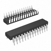
Ordering Code:
Order Number MM74C912N Package Number N28B Package Description 28-Lead Plastic Dual-In-Line Package (PDIP), JEDEC MS-010, 0.600” Wide
Connection Diagram
Dual-In-Line Package
Top View
© 1999 Fairchild Semiconductor Corporation
DS005916.prf
www.fairchildsemi.com
�MM74C912
Truth Tables
Input Control CE K3 0 0 0 0 0 0 0 0 0 0 0 0 0 0 0 0 1
X = Don’t Care
Digit Address K2 0 0 0 0 1 1 1 1 0 0 0 0 1 1 1 1 X K1 0 0 1 1 0 0 1 1 0 0 1 1 0 0 1 1 X
WE
Operation
0 0 0 0 0 0 0 0 1 1 1 1 1 1 1 1 X
0 1 0 1 0 1 0 1 0 1 0 1 0 1 0 1 X
Write Digit 1 Latch Digit 1 Write Digit 2 Latch Digit 2 Write Digit 3 Latch Digit 3 Write Digit 4 Latch Digit 4 Write Digit 5 Latch Digit 5 Write Digit 6 Latch Digit 6 Write Null Digit Latch Null Digit Write Null Digit Latch Null Digit Disable Writing
Output Control SOE 0 0 1 1 OSE 0 1 0 1 Refresh Display Stop Oscillator (Note 1) Disable Segment Outputs Standby Mode Operation
Note 1: Segment drive may exceed maximum display dissipation.
www.fairchildsemi.com
2
�MM74C912
Functional Description
Character Font
Segment Identification
The MM74C912 display controller is manufactured using metal gate CMOS technology. A single 5V 74 series TTL supply can be used for power and should be bypassed at the VCC pin. All inputs are TTL compatible; the segment outputs drive the LED display directly through current limiting resistors. The digit outputs are designed to directly drive the base of
a grounded emitter digit transistor without the need of a Darlington configuration. As seen in the block diagram, these display controllers contain six 5-bit registers; any one of which may be randomly written. The internal multiplexer scans the registers and refreshes the display. This combination of write only memory and self-scan display makes the display controller a “refreshing experience” for an over-burdened microprocessor.
Block Diagram
3
www.fairchildsemi.com
�MM74C912
Absolute Maximum Ratings(Note 2)
(Note 3) Voltage at Any Pin Except Inputs Voltage at Any Input Operating Temperature Range (TA) Storage Temperature Range (TS) Power Dissipation (PD) −65°C to +150°C Refer to PD MAX vs TA Graph −40°C to +85°C −0.3V to VCC + 0.3V −0.3V to +15V
Operating VCC Range Absolute Maximum (VCC) Lead Temperature (Soldering, 10 seconds)
3V to 6V 6.5V 260°C
Note 2: “Absolute Maximum Ratings” are those values beyond which the safety of the device cannot be guaranteed. Except for “Operating Range” they are not meant to imply that the device should be operated at these limits. The table of “Electrical Characteristics” provides conditions for actual device operation. Note 3: All voltages reference to ground.
DC Electrical Characteristics
Min/Max limits apply at 40°C ≤ TJ ≤ 85°C, unless otherwise noted Symbol CMOS TO CMOS VIN(1) VIN(0) IIN(1) IIN(0) ICC IOUT Logical “1” Input Voltage Logical “0” Input Voltage Logical “1” Input Current Logical “0” Input Current Supply Current 3-STATE Output Current CMOS/LPTTL INTERFACE VIN(1) VIN(0) ISH Logical “1” Input Voltage Logical “0” Input Voltage High Level Segment Current IDH High Level Digit Current VOUT(1) VOUT(0) θJA Logical “1” Output Voltage Any Digit Logical “0” Output Voltage Any Digit Thermal Resistance (Note 4) 100 °C/W
Note 4: θJA measured in free air with device soldered into printed circuit board.
Parameter VCC = 5V VCC = 5V
Conditions
Min
Typ
Max
Units
3.0 1.5 0.005 −1.0 −0.005 0.5 0.03 −10 VCC − 2.0 0.8 −0.03 2 10 1.0
V V µA µA mA µA µA V V
VCC = 5V, VIN = 15V VCC = 5V, VIN = 0V VCC = 5V, Outputs Open VCC = 5V, VO = 5V VCC = 5V, VO = 0V VCC = 4.75V VCC = 4.75V VCC = 5V, VO = 3.4V TJ = 25°C TJ = 100°C VCC = 5V, VO = 1V TJ = 25°C TJ = 100°C VCC = 5V, IO = −360µA VCC = 5V, IO = 360µA −10 −7 4.6 −60 −40
OUTPUT DRIVE −100 −60 −20 −15 mA mA mA mA V 0.4 V
www.fairchildsemi.com
4
�MM74C912
AC Electrical Characteristics
VCC = 5V, tr = tf = 20 ns, CL = 50 pF Symbol tCW tAW tWW tDW tWD tWA tWC t1H, t0H tH1, tH0 tIB fMUX CIN COUT Parameter Chip Enable to Write Enable Setup Time Address to Write Enable Setup Time Write Enable Width Data to Write Enable Setup Time Write Enable to Data Hold Time Write Enable to Address Hold Time Write Enable to Chip Enable Hold Time Logical “1”, Logical “0” Levels into 3-STATE 3-STATE to Logical “1” to Logical “0” Level Interdigit Blanking Time Multiplex Scan Frequency Input Capacitance 3-STATE Output Capacitance
(Note 5)
Conditions Min 35 50 35 50 400 450 390 430 0 0 0 0 50 75 Typ 15 20 15 20 225 250 225 250 −10 −15 −10 −15 30 40 275 325 325 375 5 10 10 20 350 250 5 30 7.5 50 500 600 600 700 Max Units ns ns ns ns ns ns ns ns ns ns ns ns ns ns ns ns ns ns µs µs Hz Hz pF pF
TJ = 25°C TJ = 125°C TJ = 25°C TJ = 125°C TJ = 25°C TJ = 125°C TJ = 25°C TJ = 125°C TJ = 25°C TJ = 125°C TJ = 25°C TJ = 125°C TJ = 25°C TJ = 125°C RL = 10k, TJ = 25°C CL = 10 pF, TJ = 125°C RL = 10k, TJ = 25°C CL = 50 pF, TJ = 125°C TJ = 25°C TJ = 125°C TJ = 25°C TJ = 125°C (Note 6) (Note 6)
Note 5: AC Parameters are guaranteed by DC correlated testing. Note 6: C apacitance is guaranteed by periodic testing.
5
www.fairchildsemi.com
�MM74C912
Switching Time Waveforms
Multiplexing Output Waveforms
T = 1/fMUX
Typical Performance Characteristics
ISH vs VOUT IAVG vs RLIM
Segment outputs if shorted to ground will exceed maximum power dissipation of the device
VCE is the saturation voltage of the digit drive transistor.
IDH vs VOUT
Power Dissipation vs. Temperature for Plastic Packages
www.fairchildsemi.com
6
�MM74C912
Typical Applications
Digit Output Structure Segment Output Structure
Input Protection
7
www.fairchildsemi.com
�MM74C912 6-Digit BCD Display Controller/Driver
Physical Dimensions inches (millimeters) unless otherwise noted
28-Lead Plastic Dual-In-Line Package (PDIP), JEDEC MS-010, 0.600” Wide Package Number N28B
LIFE SUPPORT POLICY FAIRCHILD’S PRODUCTS ARE NOT AUTHORIZED FOR USE AS CRITICAL COMPONENTS IN LIFE SUPPORT DEVICES OR SYSTEMS WITHOUT THE EXPRESS WRITTEN APPROVAL OF THE PRESIDENT OF FAIRCHILD SEMICONDUCTOR CORPORATION. As used herein: 2. A critical component in any component of a life support 1. Life support devices or systems are devices or systems device or system whose failure to perform can be reawhich, (a) are intended for surgical implant into the sonably expected to cause the failure of the life support body, or (b) support or sustain life, and (c) whose failure device or system, or to affect its safety or effectiveness. to perform when properly used in accordance with instructions for use provided in the labeling, can be reasonably expected to result in a significant injury to the www.fairchildsemi.com user.
Fairchild does not assume any responsibility for use of any circuitry described, no circuit patent licenses are implied and Fairchild reserves the right at any time without notice to change said circuitry and specifications.
�