MM74HC00N

MM74HC00N

  • 厂商:

    FAIRCHILD(仙童半导体)

  • 封装:

  • 描述:

    MM74HC00N - Quad 2-Input NAND Gate - Fairchild Semiconductor

  • 详情介绍
  • 数据手册
  • 价格&库存
MM74HC00N 数据手册
MM74HC00 Quad 2-Input NAND Gate September 1983 Revised January 2005 MM74HC00 Quad 2-Input NAND Gate General Description The MM74HC00 NAND gates utilize advanced silicon-gate CMOS technology to achieve operating speeds similar to LS-TTL gates with the low power consumption of standard CMOS integrated circuits. All gates have buffered outputs. All devices have high noise immunity and the ability to drive 10 LS-TTL loads. The 74HC logic family is functionally as well as pin-out compatible with the standard 74LS logic family. All inputs are protected from damage due to static discharge by internal diode clamps to VCC and ground. Features s Typical propagation delay: 8 ns s Wide power supply range: 2–6V s Low quiescent current: 20 µA maximum (74HC Series) s Low input current: 1 µA maximum s Fanout of 10 LS-TTL loads Ordering Code: Order Number MM74HC00M MM74HC00MX_NL MM74HC00SJ MM74HC00MTC MM74HC00MTCX_NL MM74HC00N MM74HC00N_NL Package Number M14A M14A M14D MTC14 MTC14 N14A N14A Package Description 14-Lead Small Outline Integrated Circuit (SOIC), JEDEC MS-012, 0.150" Narrow Pb-Free 14-Lead Small Outline Integrated Circuit (SOIC), JEDEC MS-012, 0.150" Narrow Pb-Free 14-Lead Small Outline Package (SOP), EIAJ TYPE II, 5.3mm Wide 14-Lead Thin Shrink Small Outline Package (TSSOP), JEDEC MO-153, 4.4mm Wide Pb-Free 14-Lead Thin Shrink Small Outline Package (TSSOP), JEDEC MO-153, 4.4mm Wide 14-Lead Plastic Dual-In-Line Package (PDIP), JEDEC MS-001, 0.300" Wide Pb-Free 14-Lead Plastic Dual-In-Line Package (PDIP), JEDEC MS-001, 0.300" Wide Devices also available in Tape and Reel. Specify by appending the suffix letter “X” to the ordering code. Pb-Free package per JEDEC J-STD-020B. Connection Diagram Pin Assignments for DIP, SOIC, SOP and TSSOP Logic Diagram Top View © 2005 Fairchild Semiconductor Corporation DS005292 www.fairchildsemi.com MM74HC00 Absolute Maximum Ratings(Note 1) (Note 2) Supply Voltage (VCC) DC Input Voltage (VIN) DC Output Voltage (VOUT) Clamp Diode Current (IIK, IOK) DC Output Current, per pin (IOUT) DC VCC or GND Current, per pin (ICC) Storage Temperature Range (TSTG) Power Dissipation (PD) (Note 3) S.O. Package only Lead Temperature (TL) (Soldering 10 seconds) 260°C 600 mW 500 mW Recommended Operating Conditions Min Supply Voltage (VCC) DC Input or Output Voltage (VIN, VOUT) Operating Temperature Range (TA) Input Rise or Fall Times (tr, tf) VCC = 2V VCC = 4.5V VCC = 6.0V 1000 500 400 ns ns ns 2 0 Max 6 VCC Units V V −0.5 to +7.0V −1.5 to VCC+1.5V −0.5 to VCC+0.5V ±20 mA ±25 mA ±50 mA −65°C to +150°C −40 +85 °C Note 1: Absolute Maximum Ratings are those values beyond which damage to the device may occur. Note 2: Unless otherwise specified all voltages are referenced to ground. Note 3: Power Dissipation temperature derating — plastic “N” package: − 12 mW/°C from 65°C to 85°C. DC Electrical Characteristics Symbol VIH Parameter Minimum HIGH Level Input Voltage VIL Maximum LOW Level Input Voltage VOH Minimum HIGH Level Output Voltage VIN = VIH or VIL |IOUT| ≤ 20 µA Conditions (Note 4) VCC 2.0V 4.5V 6.0V 2.0V 4.5V 6.0V 2.0V 4.5V 6.0V 2.0 4.5 6.0 4.2 5.7 0 0 0 0.2 0.2 TA = 25°C Typ 1.5 3.15 4.2 0.5 1.35 1.8 1.9 4.4 5.9 3.98 5.48 0.1 0.1 0.1 0.26 0.26 ±0.1 2.0 TA = −40 to 85°C TA = −55 to 125°C Guaranteed Limits 1.5 3.15 4.2 0.5 1.35 1.8 1.9 4.4 5.9 3.84 5.34 0.1 0.1 0.1 0.33 0.33 ±1.0 20 1.5 3.15 4.2 0.5 1.35 1.8 1.9 4.4 5.9 3.7 5.2 0.1 0.1 0.1 0.4 0.4 ±1.0 40 Units V V V V V V V V V V V V V V V V µA µA VIN = VIH or VIL |IOUT| ≤ 4.0 mA |IOUT| ≤ 5.2 mA VOL Maximum LOW Level Output Voltage VIN = VIH |IOUT| ≤ 20 µA 2.0V 4.5V 6.0V VIN = VIH |IOUT| ≤ 4.0 mA |IOUT| ≤ 5.2 mA IIN ICC Maximum Input Current Maximum Quiescent Supply Current VIN = VCC or GND IOUT = 0 µA 6.0V VIN = VCC or GND 4.5V 6.0V 6.0V 4.5V 6.0V Note 4: For a power supply of 5V ±10% the worst case output voltages (VOH, and VOL) occur for HC at 4.5V. Thus the 4.5V values should be used when designing with this supply. Worst case VIH and VIL occur at VCC = 5.5V and 4.5V respectively. (The VIH value at 5.5V is 3.85V.) The worst case leakage current (IIN, ICC, and IOZ) occur for CMOS at the higher voltage and so the 6.0V values should be used. www.fairchildsemi.com 2 MM74HC00 AC Electrical Characteristics VCC = 5V, TA = 25°C, CL = 15 pF, tr = tf = 6 ns Symbol tPHL, tPLH Parameter Maximum Propagation Delay Conditions Typ 8 Guaranteed Limit 15 Units ns AC Electrical Characteristics VCC = 2.0V to 6.0V, CL = 50 pF, tr = tf = 6 ns (unless otherwise specified) Symbol Parameter Conditions VCC 2.0V 4.5V 6.0V tTLH, tTHL Maximum Output Rise and Fall Time CPD CIN Power Dissipation Capacitance (Note 5) Maximum Input Capacitance Note 5: CPD determines the no load dynamic power consumption, PD = CPD VCC2 f + ICC VCC, and the no load dynamic current consumption, IS = CPD VCC f + ICC. TA = 25°C Typ 45 9 8 30 8 7 20 5 10 90 18 15 75 15 13 TA = −40 to 85°C TA = −55 to 125°C Guaranteed Limits 113 23 19 95 19 16 134 27 23 110 22 19 Units ns ns ns ns ns ns pF tPHL, tPLH Maximum Propagation Delay 2.0V 4.5V 6.0V (per gate) 10 10 pF 3 www.fairchildsemi.com MM74HC00 Physical Dimensions inches (millimeters) unless otherwise noted 14-Lead Small Outline Integrated Circuit (SOIC), JEDEC MS-012, 0.150" Narrow Package Number M14A www.fairchildsemi.com 4 MM74HC00 Physical Dimensions inches (millimeters) unless otherwise noted (Continued) Pb-Free 14-Lead Small Outline Package (SOP), EIAJ TYPE II, 5.3mm Wide Package Number M14D 5 www.fairchildsemi.com MM74HC00 Physical Dimensions inches (millimeters) unless otherwise noted (Continued) 14-Lead Thin Shrink Small Outline Package (TSSOP), JEDEC MO-153, 4.4mm Wide Package Number MTC14 www.fairchildsemi.com 6 MM74HC00 Quad 2-Input NAND Gate Physical Dimensions inches (millimeters) unless otherwise noted (Continued) 14-Lead Plastic Dual-In-Line Package (PDIP), JEDEC MS-001, 0.300" Wide Package Number N14A Fairchild does not assume any responsibility for use of any circuitry described, no circuit patent licenses are implied and Fairchild reserves the right at any time without notice to change said circuitry and specifications. LIFE SUPPORT POLICY FAIRCHILD’S PRODUCTS ARE NOT AUTHORIZED FOR USE AS CRITICAL COMPONENTS IN LIFE SUPPORT DEVICES OR SYSTEMS WITHOUT THE EXPRESS WRITTEN APPROVAL OF THE PRESIDENT OF FAIRCHILD SEMICONDUCTOR CORPORATION. As used herein: 1. Life support devices or systems are devices or systems which, (a) are intended for surgical implant into the body, or (b) support or sustain life, and (c) whose failure to perform when properly used in accordance with instructions for use provided in the labeling, can be reasonably expected to result in a significant injury to the user. 7 2. A critical component in any component of a life support device or system whose failure to perform can be reasonably expected to cause the failure of the life support device or system, or to affect its safety or effectiveness. www.fairchildsemi.com www.fairchildsemi.com
MM74HC00N
物料型号: - MM74HC00M:14-Lead Small Outline Integrated Circuit (SOIC), JEDEC MS-012, 0.150" Narrow - MM74HC00MX_NL:Pb-free 14-Lead Small Outline Integrated Circuit (SOIC), JEDEC MS-012, 0.150" Narrow - MM74HC00SJ:Pb-free 14-Lead Small Outline Package (SOP), EIAJ TYPE II, 5.3mm Wide - MM74HC0OMTC:14-Lead Thin Shrink Small Outline Package (TSSOP), JEDEC MO-153, 4.4mm Wide - MM74HCOOMTCX_NL:Pb-free 14-Lead Thin Shrink Small Outline Package (TSSOP), JEDEC MO-153, 4.4mm Wide - 
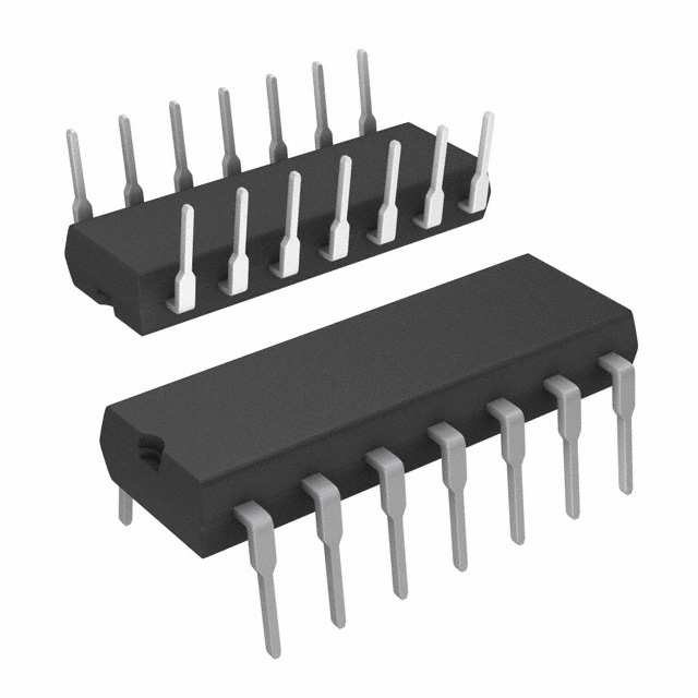
MM74HCOON:14-Lead Plastic Dual-In-Line Package (PDIP), JEDEC MS-001, 0.300" Wide - MM74HCOON NL:Pb-free 14-Lead Plastic Dual-In-Line Package (PDIP), JEDEC MS-001, 0.300" Wide

器件简介: MM74HC00是一种四2输入NAND门集成电路,采用先进的硅门CMOS技术,实现与LS-TTL门相似的运行速度,同时保持标准CMOS集成电路的低功耗。所有门都有缓冲输出,具有高噪声免疫力,能够驱动10个LS-TTL负载。74HC系列在功能和引脚排列上与标准74LS逻辑系列兼容。所有输入都通过内部二极管夹到VCC和地保护,以防静电放电损坏。

引脚分配: 文档提供了DIP, SOIC, SOP和TSSOP的连接图和逻辑图,展示了各个引脚的分配。

参数特性: - 典型传播延迟:8ns - 宽电源电压范围:2-6V - 低静态电流:最大20µA(74HC系列) - 低输入电流:最大1µA,扇出10个LS-TTL负载

功能详解: MM74HC00包含四个2输入NAND门,每个门的输出为低电平,仅当两个输入都为高电平时输出才为高电平。

应用信息: 该器件适用于需要高速和低功耗逻辑功能的场合,如数字电路、计算机系统等。

封装信息: - SOIC封装:14引脚小外形集成电路封装,JEDEC MS-012标准,0.150"窄体 - SOP封装:14引脚小外形封装,EIAJ TYPE II标准,5.3mm宽体 - TSSOP封装:14引脚薄型缩减小外形封装,JEDEC MO-153标准,4.4mm宽体 - PDIP封装:14引脚塑料双列直插封装,JEDEC MS-001标准,0.300"宽体
MM74HC00N 价格&库存

很抱歉,暂时无法提供与“MM74HC00N”相匹配的价格&库存,您可以联系我们找货

免费人工找货