Revised September 2001
MM74HC148
8-3 Line Priority Encoder
General Description
Features
The MM74HC148 priority encoder utilizes advanced silicon-gate CMOS technology. It has the high noise immunity
and low power consumption typical of CMOS circuits, as
well as the speeds and output drive similar to LB-TTL.
■ Typical propagation delay: 13 ns
■ Wide supply voltage range: 2V–6V
This priority encoder accepts 8 input request lines 0–7 and
outputs 3 lines A0–A2. The priority encoding ensures that
only the highest order data line is encoded. Cascading circuitry (enable input EI and enable output EO) has been
provided to allow octal expansion without the need for
external circuitry. All data inputs and outputs are active at
the low logic level.
All inputs are protected from damage due to static discharge by internal diode clamps to VCC and ground.
Ordering Code:
Order Number
Package Number
Package Description
MM74HC148M
M16A
16-Lead Small Outline Integrated Circuit (SOIC), JEDEC MS-012, 0.150" Narrow
MM74HC148N
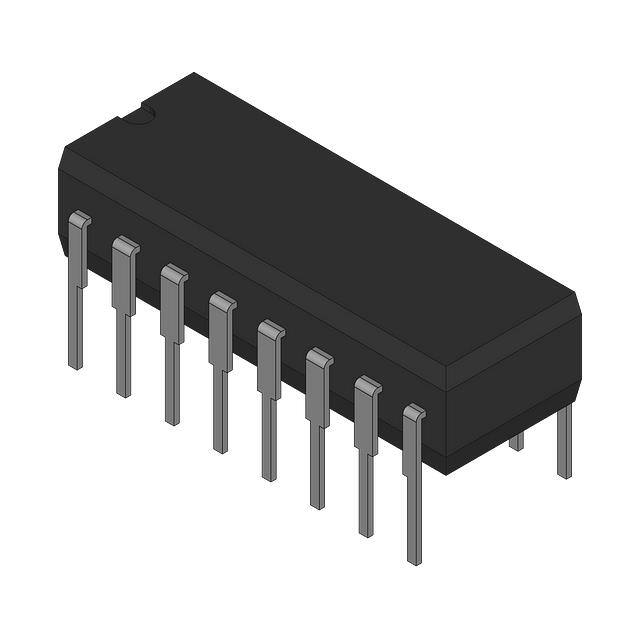
N16E
16-Lead Plastic Dual-In-Line Package (PDIP), JEDEC MS-001, 0.300" Wide
Connection Diagram
Truth Table
Inputs
EI
0
1
2
3
Outputs
4
5
6
7 A2 A1 A0 GS EO
H
X X X X X X X X
H
H
H
H
L
H H H H H H H H
H
H
H
H
H
L
L
X X X X X X X L
L
L
L
L
H
L
X X X X X X L H
L
L
H
L
H
L
X X X X X L H H
L
H
L
L
H
L
X X X X L H H H
L
H
H
L
H
L
X X X L H H H H
H
L
L
L
H
L
X X L H H H H H
H
L
H
L
H
L
X L H H H H H H
H
H
L
L
H
L
L H H H H H H H
H
H
H
L
H
H = HIGH
L = LOW
X = Irrelevant
© 2001 Fairchild Semiconductor Corporation
DS009390
www.fairchildsemi.com
MM74HC148 8-3 Line Priority Encoder
October 1987
�MM74HC148
Schematic Diagram
www.fairchildsemi.com
2
�MM74HC148
Logic Diagram
3
www.fairchildsemi.com
�MM74HC148
Absolute Maximum Ratings(Note 1)
Operation Conditions
(Note 2)
−0.5 to +7.0V
Supply Voltage (VCC)
DC Input Voltage (VIN)
−1.5 to VCC +1.5V
DC Output Voltage (VOUT)
−0.5 to VCC +0.5V
Clamp Diode Current (IIK, IOK)
±20 mA
DC Output Current, per pin (IOUT)
±25 mA
DC VCC or GND Current, per pin (ICC)
±50 mA
600 mW
S.O. Package only
500 mW
V
DC Input or Output Voltage
0
VCC
V
MM74HC
−40
+85
°C
MM54HC
−55 +125
°C
Input Rise or Fall Times
(tr, tf)
Lead Temperature (TL)
VCC = 2.0V
1000
ns
VCC = 4.5V
500
ns
VCC = 6.0V
400
ns
Note 1: Absolute Maximum Ratings are those values beyond which damage to the device may occur.
260°C
(Soldering 10 sec.)
Units
6
Operating Temperature Range (TA)
Power Dissipation (PD)
(Note 3)
Max
2
(VIN, VOUT)
−65°C to +150°C
Storage Temperature Range (TSTG)
Min
Supply Voltage (VCC)
Note 2: Unless otherwise specified all voltages are referenced to ground.
Note 3: Power Dissipation temperature derating—plastic “N” package: −12
mW/°C from 65°C to 85°C.
DC Electrical Characteristics
Symbol
VIH
VIL
VOH
Parameter
(Note 4)
VCC
Conditions
TA = 25°C
Typ
TA = −40 to 85°C
TA = −55 to 125°C
Guaranteed Limits
Units
Minimum HIGH Level
2.0V
1.5
1.5
1.5
Input Voltage
4.5V
3.15
3.15
3.15
V
V
6.0V
4.2
4.2
4.2
V
V
Maximum LOW Level
2.0V
0.5
0.5
0.5
Input Voltage (Note 5)
4.5V
1.35
1.35
1.35
V
6.0V
1.8
1.8
1.8
V
Minimum HIGH Level
VIN = VIH or VIL
Output Voltage
|IOUT| ≤ 20 µA
2.0V
2.0
1.9
1.9
1.9
V
4.5V
4.5
4.4
4.4
4.4
V
6.0V
6.0
5.9
5.9
5.9
V
|IOUT| ≤ 4.0 mA
4.5V
4.7
3.96
3.84
3.7
V
|IOUT| ≤ 5.2 mA
6.0V
5.2
5.48
5.34
5.2
V
VIN = VIH or VIL
VOL
Maximum LOW Level
VIN = VIH or VIL
Output Voltage
|IOUT| ≤ 20 µA
2.0V
0
0.1
0.1
0.1
V
4.5V
0
0.1
0.1
0.1
V
6.0V
0
0.1
0.1
0.1
V
|IOUT| ≤ 4.0 mA
4.5V
0.2
0.26
0.33
0.4
V
|IOUT| ≤ 5.2 mA
6.0V
0.2
0.26
0.33
0.4
V
VIN = VCC or GND
6.0V
±0.1
±1.0
±1.0
µA
Maximum Quiescent
VIN = VCC or GND
6.0V
8.0
80
160
µA
Supply Current
IOUT = 0 µA
VIN = VIH or VIL
IIN
ICC
Maximum Input Current
Note 4: For a power supply of 5V ±10% the worst case output voltages (VOH, and VOL) occur for HC at 4.5V. Thus the 4.5V values should be used when
designing with this supply. Worst case VIH and VIL occur at VCC = 5.5V and 4.5V respectively. (The VIH value at 5.5V is 3.85V.) The worst case leakage current (IIN, ICC, and IOZ) occur for CMOS at the higher voltage and so the 6.0V values should be used.
Note 5: VIL limits are currently tested at 20% of VCC.
www.fairchildsemi.com
4
�Symbol
tPHL, tPLH
Parameter
Conditions
Maximum Propagation Delay,
Typ
Guaranteed Limits
14
Units
ns
Any Input to Any Output
AC Electrical Characteristics
VCC = 2.0V to 6.0V, CL = 50 pF, tr = tf = 6 ns (unless otherwise specified)
Symbol
tPHL, tPLH
tPHL, tPLH
tPHL, tPLH
tPHL, tPLH
tPHL, tPLH
tPHL, tPLH
tf, tr
Cpd
Parameter
VCC
Inputs 0–7
2.0V
to Outputs
4.5V
TA = 25°C
Typ
−40°C to +85°C
−55°C to +125°C
Guaranteed Limits
14
Units
140
175
210
ns
28
35
42
ns
A0, A1, A2
6.0V
24
30
36
ns
Inputs 0–7
2.0V
140
175
210
ns
to
4.5V
28
35
42
ns
Output EO
6.0V
24
30
36
ns
Inputs 0–7
2.0V
160
200
240
ns
to
4.5V
32
40
48
ns
Output GS
6.0V
27
34
41
ns
160
200
240
ns
32
40
48
ns
Input EI
2.0V
to Outputs
4.5V
15
17
17
A0, A1, A2
6.0V
27
34
41
ns
Input EI
2.0V
100
125
150
ns
to
4.5V
20
25
30
ns
Output GS
6.0V
17
21
26
ns
100
125
150
ns
20
25
30
ns
12
Input EI
2.0V
to
4.5V
Output EO
6.0V
17
21
26
ns
Maximum
2.0V
75
95
110
ns
Output Rise
4.5V
and Fall Time
6.0V
Power Dissipation
12
7
15
19
22
ns
13
16
19
ns
52
pF
Capacitance (Note 6)
Cin
Maximum Input
5
10
10
10
pF
Capacitance
Note 6: Cpd determines the no load dynamic power consumption, and the no load dynamic current consumption.
5
www.fairchildsemi.com
MM74HC148
AC Electrical Characteristics
�MM74HC148
Physical Dimensions inches (millimeters) unless otherwise noted
16-Lead Small Outline Integrated Circuit (SOIC), JEDEC MS-012, 0.150" Narrow
Package Number M16A
www.fairchildsemi.com
6
�MM74HC148 8-3 Line Priority Encoder
Physical Dimensions inches (millimeters) unless otherwise noted (Continued)
16-Lead Plastic Dual-In-Line Package (PDIP), JEDEC MS-001, 0.300" Wide
Package Number N16E
Fairchild does not assume any responsibility for use of any circuitry described, no circuit patent licenses are implied and
Fairchild reserves the right at any time without notice to change said circuitry and specifications.
LIFE SUPPORT POLICY
FAIRCHILD’S PRODUCTS ARE NOT AUTHORIZED FOR USE AS CRITICAL COMPONENTS IN LIFE SUPPORT
DEVICES OR SYSTEMS WITHOUT THE EXPRESS WRITTEN APPROVAL OF THE PRESIDENT OF FAIRCHILD
SEMICONDUCTOR CORPORATION. As used herein:
2. A critical component in any component of a life support
device or system whose failure to perform can be reasonably expected to cause the failure of the life support
device or system, or to affect its safety or effectiveness.
1. Life support devices or systems are devices or systems
which, (a) are intended for surgical implant into the
body, or (b) support or sustain life, and (c) whose failure
to perform when properly used in accordance with
instructions for use provided in the labeling, can be reasonably expected to result in a significant injury to the
user.
www.fairchildsemi.com
7
www.fairchildsemi.com
�
很抱歉,暂时无法提供与“MM74HC148N”相匹配的价格&库存,您可以联系我们找货
免费人工找货