### 物料型号
- Order Number: NC7SP38P5X, NC7SP38L6X
- Package Number: MAA05A, MAC06A
- Product Code Top Mark: 938, K7
- Package Description:
- 5-Lead SC70, EIAJ SC-88a, 1.25mm Wide
- 6-Lead MicroPak, 1.0mm Wide
- Supplied As: 3k Units on Tape and Reel, 5k Units on Tape and Reel
### 器件简介
NC7SP38是一款由Fairchild生产的2输入NAND门(开漏输出级),属于Ultra Low Power (ULP)系列的TinyLogic。该产品适用于电池寿命至关重要的应用场合,设计用于0.9V至3.6V的供电范围内实现超低功耗。
### 引脚分配
- SC70:
- A, B: 输入
- Y: 输出
- NC: 无连接
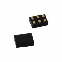
- MicroPak:
- 具体引脚图未提供,但通常为2个输入和1个输出,其余为电源和地或无连接。
### 参数特性
- 供电范围: 0.9V至3.6V
- 过压容忍: 3.6V
- 典型传播延迟: 0.9V时24ns,3.0V至3.6V时3.0ns,2.3V至2.7V时4.0ns,1.65V至1.95V时5.0ns,1.40V至1.60V时6.0ns,1.10V至1.30V时9.0ns。
- 静态驱动电流: 0.9V时±20µA,1.10V至1.30V时±0.5mA,1.40V至1.60V时±1mA,1.65V至1.95V时±1.5mA,2.3V至2.7V时±2.1mA,3.00V时±2.6mA。
- 使用专利Quiet Series降噪/EMI降低电路技术。
### 功能详解
NC7SP38是一个单一的2输入NAND门,具有开漏输出级,内部电路由最少数量的反相器级组成,包括输出缓冲器,以实现超低静态和动态功耗。该产品采用先进的CMOS技术制造,以实现最佳速度操作,同时保持极低的CMOS功耗。
### 应用信息
该产品适用于电池供电的应用,如便携式设备、无线通信设备等,可以显著延长电池寿命。
### 封装信息
- SC70: 5引脚,1.25mm宽
- MicroPak: 6引脚,1.0mm宽