NC7ST00 TinyLogic HST 2-Input NAND Gate
February 1997 Revised August 2004
NC7ST00 TinyLogic HST 2-Input NAND Gate
General Description
The NC7ST00 is a single 2-Input high performance CMOS NAND Gate, with TTL-compatible inputs. Advanced Silicon Gate CMOS fabrication assures high speed and low power circuit operation. ESD protection diodes inherently guard both inputs and output with respect to the VCC and GND rails. High gain circuitry offers high noise immunity and reduced sensitivity to input edge rate. The TTL-compatible inputs facilitate TTL to NMOS/CMOS interfacing. Device performance is similar to MM74HCT but with 1/2 the output current drive of HC/HCT.
Features
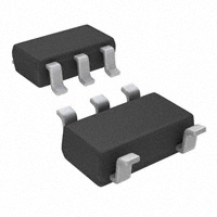
s Space saving SOT23 or SC70 5-lead package s Ultra small MicroPak leadless package s High Speed; tPD < 7 ns typ, VCC = 5V, CL = 15 pF s Low Quiescent Power; ICC < 1 µA typ, VCC = 5.5V s Balanced Output Drive; 2 mA IOL, −2 mA IOH s TTL-compatible inputs
Ordering Code:
Order Number NC7ST00M5X NC7ST00P5X NC7ST00L6X Package Number MA05B MAA05A MAC06A Product Code Top Mark 8S00 T00 E3 Package Description 5-Lead SOT23, JEDEC MO-178, 1.6mm 5-Lead SC70, EIAJ SC-88a, 1.25mm Wide 6-Lead MicroPak, 1.0mm Wide Supplied As 3k Units on Tape and Reel 3k Units on Tape and Reel 5k Units on Tape and Reel
Logic Symbol
IEEE/IEC
Connection Diagrams
Pin Assignments for SOT23 and SC70
Pin Descriptions
Pin Names A, B Y NC Description Inputs Output No Connect Pad Assignments for MicroPak (Top View)
Function Table
Y = AB Inputs A L L H H
H = HIGH Logic Level L = LOW Logic Level TinyLogic is a registered trademark of Fairchild Semiconductor Corporation. MicroPak is a trademark of Fairchild Semiconductor Corporation.
Output B L H L H Y H H H L (Top Thru View)
© 2004 Fairchild Semiconductor Corporation
DS012181
www.fairchildsemi.com
�NC7ST00
Absolute Maximum Ratings(Note 1)
Supply Voltage (VCC) DC Input Diode Current (lIK) VIN < −0.5V VIN ≥ VCC + 0.5V DC Input Voltage VIN DC Output Diode Current (IOK) VOUT < −0.5V VOUT > VCC +0.5V Output Voltage (VOUT) DC Output Source or Sink Current (IOUT) DC VCC or Ground Current per Supply Pin (ICC or IGND) Storage Temperature (TSTG) Junction Temperature (TJ) Lead Temperature (TL); (Soldering, 10 seconds) Power Dissipation (PD) @ +85°C SOT23-5 SC70-5 200 mW 150 mW 260°C
−0.5V to +7.0V −20 mA +20 mA −0.5V to VCC + 0.5V −20 mA +20 mA −0.5V to VCC + 0.5V ±12.5 mA ±25 mA −65°C to +150°C
150°C
Recommended Operating Conditions (Note 2)
Supply Voltage Input Voltage (VIN) Output Voltage (VOUT) Operating Temperature (TA) Input Rise and Fall Time (tr, tf) VCC = 5.0V Thermal Resistance (θJA) SOT23-5 SC70-5 300°C/W 425°C/W 0 to 500 ns 4.5V to 5.5V 0.0V to VCC 0V to VCC
−40°C to +85°C
Note 1: Absolute Maximum Ratings are those values beyond which damage to the device may occur. The databook specifications should be met, without exception, to ensure that the design is reliable over its power supply, temperature, and output/input loading variables Fairchild does not recommend operation of circuits outside the databook specifications. Note 2: Unused inputs must be held HIGH or LOW. They may not float.
DC Electrical Characteristics
Symbol VIH VIL VOH Parameter HIGH Level Input Voltage LOW Level Input Voltage HIGH Level Output Voltage VCC (V) 4.5–5.5 4.5–5.5 4.5 4.5 VOL LOW Level Output Voltage 4.5 4.5 IIN ICC ICCT Input Leakage Current Quiescent Supply Current ICC per Input 5.5 5.5 5.5 4.4 4.18 4.5 4.35 0 0.10 0.1 0.26 ±0.1 1.0 2.0 Min 2.0 0.8 4.4 4.13 0.1 0.33 ±1.0 10.0 2.9 V µA µA mA V TA = +25°C Typ Max TA = −40°C to +85°C Min 2.0 0.8 Max Units V V IOH = −20 µA IOH = −2 mA VIN = VIL IOL = 20 µA IOL = 2 mA VIN = VIH 0 ≤ VIN ≤ 5.5V VIN = VCC or GND One Input VIN = 0.5V or 2.4V, Other Input VCC or GND Conditions
www.fairchildsemi.com
2
�NC7ST00
AC Electrical Characteristics
Symbol tPLH, tPHL 4.5 5.5 tTLH, tTHL CIN CPD Input Capacitance Power Dissipation Capacitance Output Transition Time 5.0 4.5 5.5 Open 5.0 Parameter Propagation Delay VCC (V) 5.0 Min TA = +25°C Typ 3.4 6.3 6.0 11.5 4.1 11.2 4 11 10 2 6 Max 12 17 16 27 14 26 10 25 21 10 31 26 20 31 18 30 ns ns pF pF (Note 3) Figure 2 CL = 15 pF CL = 50 pF Figures 1, 3 ns CL = 50 pF TA = −40°C to +85°C Min Max Units Conditions CL = 15 pF Figures 1, 3 Figure Number
Note 3: C PD is defined as the value of the internal equivalent capacitance which is derived from dynamic operating current. Current consumption (ICCD ) at no output loading and operating at 50% duty cycle. (See Figure 2). CPD is related to ICCD dynamic operating current by the expression: ICCD = (C PD)(VCC)(fIN) + (ICCstatic).
AC Loading and Waveforms
CL includes load and stray capacitance Input PRR = 1.0 MHz; tw = 500 ns
FIGURE 1. AC Test Circuit
Input = AC Waveform; PRR = variable; Duty Cycle = 50%
FIGURE 3. AC Waveforms
FIGURE 2. ICCD Test Circuit
3
www.fairchildsemi.com
�NC7ST00
Tape and Reel Specification
TAPE FORMAT Package Designator M5X, P5X Tape Section Leader (Start End) Carrier Trailer (Hub End) TAPE DIMENSIONS inches (millimeters) Number Cavities 125 (typ) 3000 75 (typ) Cavity Status Empty Filled Empty Cover Tape Status Sealed Sealed Sealed
Package SC70-5 SOT23-5
Tape Size 8 mm 8 mm
DIM A 0.093 (2.35) 0.130 (3.3)
DIM B 0.096 (2.45) 0.130 (3.3)
DIM F (3.5 ± 0.10) (3.5 ± 0.05)
DIM Ko (1.35 ± 0.10) (1.4 ± 0.11)
DIM P1 0.157 (4) 0.157 (4)
DIM W 0.315 ± 0.004 (8 ± 0.1) 0.315 ± 0.012 (8 ± 0.3)
0.138 ± 0.004 0.053 ± 0.004 0.138 ± 0.002 0.055 ± 0.004
www.fairchildsemi.com
4
�NC7ST00
Tape and Reel Specification
TAPE FORMAT for MicroPak Package Designator L6X Tape Section Leader (Start End) Carrier Trailer (Hub End)
(Continued) Number Cavities 125 (typ) 5000 75 (typ) Cavity Status Empty Filled Empty Cover Tape Status Sealed Sealed Sealed
REEL DIMENSIONS inches (millimeters)
Tape Size 8 mm
A 7.0 (177.8)
B 0.059 (1.50)
C 0.512 (13.00)
D 0.795 (20.20)
N 2.165 (55.00)
W1 0.331 + 0.059/−0.000 (8.40 + 1.50/−0.00)
W2 0.567 (14.40)
W3 W1 + 0.078/−0.039 (W1 + 2.00/−1.00)
5
www.fairchildsemi.com
�NC7ST00
Physical Dimensions inches (millimeters) unless otherwise noted
5-Lead SOT23, JEDEC MO-178, 1.6mm Package Number MA05B
www.fairchildsemi.com
6
�NC7ST00
Physical Dimensions inches (millimeters) unless otherwise noted (Continued)
5-Lead SC70, EIAJ SC-88a, 1.25mm Wide Package Number MAA05A
7
www.fairchildsemi.com
�NC7ST00 TinyLogic HST 2-Input NAND Gate
Physical Dimensions inches (millimeters) unless otherwise noted (Continued)
6-Lead MicroPak, 1.0mm Wide Package Number MAC06A
Fairchild does not assume any responsibility for use of any circuitry described, no circuit patent licenses are implied and Fairchild reserves the right at any time without notice to change said circuitry and specifications. LIFE SUPPORT POLICY FAIRCHILD’S PRODUCTS ARE NOT AUTHORIZED FOR USE AS CRITICAL COMPONENTS IN LIFE SUPPORT DEVICES OR SYSTEMS WITHOUT THE EXPRESS WRITTEN APPROVAL OF THE PRESIDENT OF FAIRCHILD SEMICONDUCTOR CORPORATION. As used herein: 1. Life support devices or systems are devices or systems which, (a) are intended for surgical implant into the body, or (b) support or sustain life, and (c) whose failure to perform when properly used in accordance with instructions for use provided in the labeling, can be reasonably expected to result in a significant injury to the user. www.fairchildsemi.com 8 2. A critical component in any component of a life support device or system whose failure to perform can be reasonably expected to cause the failure of the life support device or system, or to affect its safety or effectiveness. www.fairchildsemi.com
�
很抱歉,暂时无法提供与“NC7ST00M5X”相匹配的价格&库存,您可以联系我们找货
免费人工找货