### 物料型号
- 型号:NC7WZ38
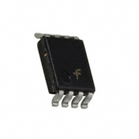
- 封装类型:
- NC7WZ38K8X:US8表面贴装封装
- NC7WZ38L8X:Pb-Free MicroPak无铅封装
### 器件简介
NC7WZ38是一款来自Fairchild的Ultra High Speed系列TinyLogic产品,具备双2输入NAND门和开漏输出级。该器件采用先进的CMOS技术制造,能够在保持低静态功耗的同时实现超高速运行和高输出驱动能力,适用于1.65V至5.5V的宽电压范围。
### 引脚分配
- An, Bn:输入引脚
- Y:输出引脚
### 参数特性
- 超高速:典型值为2.2ns的传播延迟(tPD),在5V供电下输入至50pF负载。
- 高输出灌电流:在3V供电下可达24mA。
- 宽供电电压范围:1.65V至5.5V。
- 与LCX性能匹配:在3.3V供电下运行时。
- 高阻态输入/输出:在断电状态下。
- 过压容忍输入:便于5V至3V的电平转换。
- 专利的噪声/EMI降低电路。
### 功能详解
NC7WZ38的主要功能是作为逻辑NAND门使用,其逻辑表达式为\(Y=\overline{AB}\)。当两个输入A和B都为高电平时,输出Y为低电平;否则输出为高电平或高阻态。
### 应用信息
NC7WZ38适用于需要高速逻辑运算和宽电压范围的应用场合,例如数字电路、信号处理和控制应用等。
### 封装信息
- US8封装:8引脚US8表面贴装封装,JEDEC MO-187标准,变异CA,3.1mm宽。
- MicroPak封装:Pb-Free 8引脚MicroPak封装,1.6mm宽,符合JEDEC J-STD-020B标准。


 工商网监
湘ICP备2023018690号
工商网监
湘ICP备2023018690号