RC4136M

RC4136M

  • 厂商:

    ONSEMI(安森美)

  • 封装:

    SOIC-14

  • 描述:

    OPERATIONAL AMPLIFIER

  • 详情介绍
  • 数据手册
  • 价格&库存
RC4136M 数据手册
www.fairchildsemi.com RC4136 General Performance Quad 741 Operational Amplifier Features • • • • • • • • Unity gain bandwidth – 3 MHz Short circuit protection No frequency compensation required No latch-up Large common mode and differential voltage ranges Low power consumption Parameter tracking over temperature range Gain and phase match between amplifiers Description The RC4136 is made up of four 741 type independent high gain operational amplifiers internally compensated and constructed on a single silicon chip using the planar epitaxial process. of the RC4136 quad amplifier in all 741 operational amplifier applications providing the highest possible packaging density. This amplifier meets or exceeds all specifications for 741 type amplifiers. Excellent channel separation allows the use The specially designed low noise input transistors allow the RC4136 to be used in low noise signal processing applications such as audio preamplifiers and signal conditioners. Block Diagram Pin Assignments –Input (A) +Input (A) A + D + Output (B) Output (C) + B + –Input (B) +Input (D) Output (D) Output (A) +Input (B) –Input (D) C –Input (A) +Input (A) Output (A) Output (B) +Input (B) –Input (B) –VS 1 14 2 13 3 12 4 11 5 10 6 9 7 8 –Input (D) +Input (D) Output (D) +VS Output (C) +Input (C) –Input (C) +Input (C) 65-4136-02 –Input (C) 65-4136-01 REV. 1.0.1 6/14/01 PRODUCT SPECIFICATION RC4136 Absolute Maximum Ratings (beyond which the device may be damaged)1 Parameter Supply Voltage Input Min Typ Max Units ±18 V ±30 V 30 V SOIC 300 mW PDIP 468 mW 0 70 °C -65 RC4136 Voltage2 Differential Input Voltage Output Short Circuit Duration3 PDTA < 50°C Operating Temperature Indefinite RC4136 Storage Temperature 150 °C Junction Temperature SOIC, PDIP 125 °C Lead Soldering Temperature (60 seconds) DIP 300 °C SOIC 260 °C Notes: 1. Functional operation under any of these conditions is NOT implied. Performance and reliability are guaranteed only if Operating Conditions are not exceeded. 2. For supply voltages less than ±15V, the absolute maximum input voltage is equal to the supply voltage. 3. Short circuit may be to ground, typically 45 mA. Operating Conditions Parameter θJC Thermal resistance θJA Thermal resistance For TA > 50°C Derate at 2 Min Typ Max Units 60 °C/W SOIC 200 °C/W PDIP 160 °C/W SOIC 5.0 mW/°C REV. 1.0.1 6/14/01 RC4136 PRODUCT SPECIFICATION Electrical Characteristics (VS = ±15V and TA = +25˚C, unless otherwise noted) RC4136 Parameters Test Conditions Input Offset Voltage RS ≤ 10kΩ Typ Max Units 0.5 6.0 mV Input Offset Current 5.0 200 nA Input Bias Current 40 500 nA Input Resistance Min 0.3 5.0 MΩ Large Signal Voltage Gain RL ≥ 2kΩ, VOUT = ±10V 20 300 V/mV Output Voltage Swing RL ≥ 10kΩ ±12 ±14 V RL ≥ 2kΩ ±10 ±13 ±12 ±14 V Input Voltage Range Common Mode Rejection Ratio RS ≤ 10kΩ 70 100 dB Power Supply Rejection Ratio RS ≤ 10kΩ 76 100 dB Power Consumption RL = ∞ , All Outputs 210 Rise Time VIN = 20mV, RL = 2kΩ 0.13 Overshoot CL ≤ 100pF 5.0 % 3.0 MHz 340 mW Transient Response Unity Gain Bandwidth µS Slew Rate RL ≥ 2kΩ 1.0 V/µS Channel Separation F = 1.0kHz, RS =1kΩ 90 dB Electrical Characteristics (RC = 0°C ≤ TA ≤ = 70°, VS = ± 15V) RC4136 Parameters Test Conditions Input Offset Voltage RS ≤ 10kΩ Min Typ Max Units 7.5 mV Input Offset Current 300 nA Input Bias Current 800 nA Large Signal Voltage Gain RL ≥ 2kΩ, VOUT = ±10V 15 V/mV Output Voltage Swing RL ≥ 2kΩ ±10 V Power Consumption REV. 1.0.1 6/14/01 240 400 mW 3 PRODUCT SPECIFICATION RC4136 Electrical Characteristics Comparison (VS = ±15V and TA +25˚C unless otherwise noted) Parameter RC4136 (Typ.) RC741 (Typ.) LM324 (Typ.) Units Input Offset Voltage 0.5 2.0 2.0 mV Input Offset Current 5.0 10 5.0 nA Input Bias Current 40 80 55 nA Input Resistance 5.0 2.0 Large Signal Voltage Gain (RL = 2kΩ) MΩ 300 200 100 V/mV Output Voltage Swing (RL= 2kΩ) ±13V ±13V |+VS – 1.2V| to –VS V Input Voltage Range ±14V ±13V |+VS – 1.5V| to –VS V Common Mode Rejection Ratio 100 90 85 dB Power Supply Rejection Ratio 100 90 100 dB Rise Time 0.13 0.3 µS Overshoot 5.0 5.0 % Unity Gain Bandwidth 3.0 0.8 0.8 Slew Rate 1.0 0.5 0.5 Input Noise Voltage Density (F= 1kHz) 10 22.5 nV/√Hz Short Circuit Current ±45 ±25 mA Transient Response 4 MHz V/µS REV. 1.0.1 6/14/01 RC4136 PRODUCT SPECIFICATION Typical Performance Characteristics 25 100 VS = 20 15V IOS (nA) 65-4136-03 40 20 0 0 +10 +20 +30 +40 +50 +60 15V 15 10 5 0 +70 0 +10 +20 TA (°C) +40 +50 +60 +70 TA (°C) Figure 1. Input Bias Current vs. Temperature Figure 2. Input Offset Current vs. Temperature 15 15 10 T A = +25 C 10 T A = +25 C 5 VOUT (V) 5 0 -5 65-4136-05 VCM (V) +30 -10 -15 ±4 ±6 ±8 ±10 ±12 ±14 ±16 0 -5 RL = 2 k Ω -10 -15 ±4 ±18 65-4136-06 IB (nA) 60 VS = 65-4136-04 80 ±6 ±8 ±10 ±12 ±14 ±16 ±18 +VS/-VS (V) ±VS (V) Figure 3. Input Common Mode Voltage Range vs. Supply Voltage Figure 4. Output Voltage vs. Supply Voltage 800K 240 VS = 15V VS = 15V 220 RL = 2 k Ω 0 65-4136-07 200K 0 +10 +20 +30 +40 +50 +60 TA (°C) Figure 5. Open Loop Gain vs. Temperature REV. 1.0.1 6/14/01 +70 200 180 65-4136-08 400K PC (mW) AVOL (V/mV) 600K 160 0 +10 +20 +30 +40 +50 +60 +70 TA (°C) Figure 6. Power Consumption vs. Temperature 5 PRODUCT SPECIFICATION RC4136 Typical Performance Characteristics (continued) 120 40 36 32 28 24 20 16 12 8 4 0 100 VOUT P-P (V) 60 40 65-4136-09 20 0 -20 1 10 100 1K 10K 100K 1M 10M VS = 15V T A = +25 C RL = 2 k Ω 1K 10K F (Hz) 10 TA = +25°C VS = 15V TA = +25 C IQ (mA) 8 1.0 6 4 65-4136-12 28 26 24 22 20 18 16 14 12 10 8 0.1 2 0 10 0 ±3 ±6 ±9 ±12 ±15 ±18 +VS/-VS (V) RL (kΩ) Figure 9. Output Voltage Swing vs. Load Resistance Figure 10. Quiescent Current vs. Supply Voltage 28 10 8 6 4 2 0 -2 -4 -6 -8 -10 24 VS = 15V TA = +25 C 20 VOUT (mV) Output Input 65-4136-13 VOUT (V) 1M Figure 8. Output Voltage Swing vs. Frequency 65-4136-11 VOUT P-P (V) Figure 7. Open Loop Gain vs. Frequency 0 10 20 30 Time (µS) 40 Figure 11. Follower Large Signal Pulse Response 6 100K F (Hz) 16 12 VS = 15V T A = +25 C RL = 2 k Ω C L = 100 pF 90% 8 4 65-4136-14 AVOL (dB) 80 65-4136-10 100 10% Rise Time 0 0 0.25 0.50 0.75 1.00 1.25 Time (µS) Figure 12. Transient Response Output Voltage vs. Time REV. 1.0.1 6/14/01 RC4136 PRODUCT SPECIFICATION Typical Performance Characteristics (continued) 120 0.6 100 0.5 THD (%) 80 60 65-4136-15 0 10 0.4 0.3 0.2 40 20 VOUT = 1 VRMS VS = 30V VS = 15V TA = +25 C 100 1K 10K 65-4136-16 CS (dB) 140 0.1 0 10 100K 100 1K 100K F (Hz) F (Hz) Figure 13. Channel Separation vs. Frequency 0.6 Figure 14. Total Harmonic Distortion vs. Frequency VS = 15V R L = 2K A V = 40 dB f = 1 kHz RS = 1k Ω 0.5 THD (%) 10K 0.4 0.3 65-4136-17 0.2 0.1 0 1 2 3 4 5 6 7 8 9 10 VOUT (V RMS ) Figure 15. Total Harmonic Distortion vs. Output Voltage REV. 1.0.1 6/14/01 7 PRODUCT SPECIFICATION RC4136 RC4136 Versus LM324 Although the LM324 is an excellent device for single-supply applications where ground sensing is important, it is a poor substitute for four 741s in split supply circuits. The simplified input circuit of the RC4136 exhibits much lower noise than that of the LM324 and exhibits no crossover distortion as compared with the LM324 (see Figure 16). The LM324 shows significant crossover distortion and pulse delay in attempting to handle a large signal input pulse. 324 4136 F = 10 kHz VOUT = 8 VP-P F = 50 kHz V OUT = 8 V P-P RL = 2 k Ω AV= 1 VS = 5V 65-4136-18 120 741 324 1K 10K 100K 4136 80 4136 741 60 40 1M Figure 17. Output Voltage Swing vs. Frequency 65-4136-20 20 F (Hz) 8 100 VS = 15V T A = +25 C R L = 2 kΩ AVOL (dB) 40 36 32 28 24 20 16 12 8 4 0 100 65-4136-19 VOUT P-P (V) Figure 16. Comparative Crossover Distortion 0 -20 1 10 100 1K 10K 100K 1M 10M F (Hz) Figure 18. Open Loop Gain vs. Frequency REV. 1.0.1 6/14/01 RC4136 PRODUCT SPECIFICATION RC4136 Versus LM324 (continued) +8 16 4136 +2 Outputs 0 324 -2 Input 65-4136-21 -4 -6 -8 30 0 40 60 0 C = T A < +70 C 12 +VCM (V) VOUT (V) +4 14 Vs = 10V RL = 2 kΩ 80 10 741 8 4136 6 4 65-4136-22 +6 2 0 ±5 ±10 Time (µS) ±20 ±15 +VS/-VS (V) Figure 19. Follower Large Signal Pulse Response Output Voltage vs. Time Figure 20. Input Common Mode Voltage Range vs. Supply Voltage Typical Applications +Vs 910K +Vs +Vs 1 1 2 4136A 100Ω 3 4136A 100K 3 2 VOUT 91K 5K 100K AV = 10 65-0520 +VIN Figure 21. Lamp Driver Figure 22. Power Amplifier VIN 1 2 4136A VIN VOUT 65-0519 Figure 23. Voltage Follower REV. 1.0.1 6/14/01 2 10K 3 65-0523 +VREF 1 4136A 3 VOUT 10M 65-0522 Figure 24. Comparator with Hysteresis 9 PRODUCT SPECIFICATION RC4136 Typical Applications (continued) +Vs VIN 0.01µF 16K 100K VOUT 0.001µF 1 16K 1 0.01µF 2 4136A 3 4136A 3 VoUT 2 +Vs 100K 100K 1 0 100K 100K 100K 65-0527 65-0521 Figure 25. DC Coupled 1kHz Lowpass Active Filter VIN Figure 26. Squarewave Oscillator 0.01 µF 390K 120K 0.01 µF +Vs 1 620K 620Ω VoUT 390K +Vs 4136A 3 39K 6 2 4 4136B 5 10 µF 100K 100K +Vs 65-0526 Figure 27. 1kHz Bandpass Active Filter 1M 100K +Vs +Vs 1 VIN 2 4136A 3 10K VIN VoUT +Vs 100K 100K 1 2 4136A 3 VoUT 10K 100K 0.1 µF 10 µF 100K +Vs 10 µF 10K 100K 10K 65-0525 65-0524 Figure 28. AC Coupled Non-Inverting Amplifier 10 Figure 29. AC Coupled Inverting Amplifier REV. 1.0.1 6/14/01 RC4136 PRODUCT SPECIFICATION Typical Applications (continued) 0.05 µF R 100K 100K 1 +VC* 51K 2 4136A 51K 3 6 5 4 Output 1 V+/210K 51K R/2 50K 4136B Output 2 10K 65-0528 * Wide control voltage range: 0V < Vc < 2(+Vs -1.5V) Figure 30. Voltage Control Oscillator (VCO) 2.5K Cal 20K 1% 20K 1% DC Output 20K 1% 4.7 µF AC Input 20K 1% 10K 1% 4.7 µF D1 FD666 1 2 4136A D2 FD666 4.7 µF 6 3 5 4136B 4 5.1K 10K 65-0531 Figure 31. Full-Wave Rectifier and Averaging Filter R2 30K 10K 1 4136A 3 2 R1 R3 = R2 2R4 6 C1 5 4136B 4 100 R4 7.5K 10 0.0001 C2 1 µF 65-0529 Figure 32. Notch Filter Using the RC4136 as a Gyrator REV. 1.0.1 6/14/01 1K Trim R, such that R3 15K R4 7.5K 741 Output 65-0530 Input C1 ( µF) R1 30K 0.001 0.001 0.01 1.0 Center Frequency (Hz) Figure 33. Notch Frequency vs. C1 11 PRODUCT SPECIFICATION RC4136 Typical Applications (continued) 2 V IN 1 V4 4136A 3 VIN < V4 Q1 5 6 4136B V3 4 V3 < VIN < V4 Q2 9 8 V2 4136C 10 V2 < V IN < V3 Q3 13 V1 14 4136D 12 V IN < V1 65-0532 Figure 34. Multiple Aperture Window Discriminator (-) 2 1 4136A 3 R1 45K 1% R3 10K 1% Inputs (+) 5 6 4136B 4136C VOUT * Matching determines CMRR 10 Av = R5* 10K 0.1% 4 R1 = R4 R2 = R5 R6 = R7 R4 45K 1% 8 9 R6* 100K 0.1% R2 10K 0.1% R6 2R1 (1+ ) R2 R3 R7* 100K 0.1% 65-0533 Figure 35. Differential Input Instrumentation Amplifier with High Common Mode Rejection 12 REV. 1.0.1 6/14/01 RC4136 PRODUCT SPECIFICATION Typical Applications (continued) +15V 10K 10K VIN1 D4 IN457 Q1* 10K 10K 1 2 1K 3 4136A 6 D1 1N457 10K 4 4136B 5 VoUT = (VIN1) (VIN2) VIN3 10K Q4* Q2* V IN2 10K Q3* 1K 10 9 10K 14 8 12 4136C 1K D2 1N457 10K 4136D VIN3 13 D3 1N457 10K 65-0534 *Matched Transistors Figure 36. Analog Multiplier/Divider DC-1Hz N Out 3.3M 49.9K 0.082 µF 100K 49.9Ω 1.0 µF 2 DUT 100K 49.9Ω 499K Compensate as Required 1 4136A 499K 3 60 dB Wideband Amplifier 78.7K 10 µF 1 Hz 499Ω 1 µF 1000 µF 0.1 µF 0.01 µF 1 kHz 10 µF 1 Hz 3.16K 1 Hz 3.16K 499K 10K Spot Noise Out 1 µF 8 10 6 31.6K 4136C 4 9 4136B 0.1 µF 5 100K 1mV = 1nV/ Hz RMS 499Ω 0.01 µF 1 kHz 499K Stepped 10 dB Attenuator 1 kHz Selectable Frequency Constant Q Filter 65-0535 Figure 37. Spot Noise Measurement Test Circuit REV. 1.0.1 6/14/01 13 PRODUCT SPECIFICATION RC4136 Simplified Schematic Diagram +Vs (11) R1 8.7K Q10 Q5 Q6 Q14 (1,6,8,14) -Input Q13 Q2 Q1 R6 50 R8 100 Output (3,4,10,12) Q12 +Input D1 (2,5,9,13) R7 50 R5 50K Q15 Q7 Q8 15 pF Q9 Q3 Q4 Q11 R9 15K R2 5K C1 30 pF R3 5K Z1 5.5V R4 50K -Vs (7) 65-0495 14 REV. 1.0.1 6/14/01 RC4136 PRODUCT SPECIFICATION Mechanical Dimensions (continued) 14-Lead Plastic DIP Package Inches Symbol Min. A A1 A2 Millimeters Max. Min. .210 — .195 .014 .022 .045 .070 .008 .015 .725 .795 .005 — .300 .325 .240 .280 .100 BSC — .430 .115 .200 14 — .38 2.93 — .015 .115 B B1 C D D1 E E1 e eB L N Notes: Notes Max. 5.33 — 4.95 .36 .56 1.14 1.78 .20 .38 18.42 20.19 .13 — 7.62 8.26 6.10 7.11 2.54 BSC — 10.92 2.92 5.08 14 1. Dimensioning and tolerancing per ANSI Y14.5M-1982. 2. "D" and "E1" do not include mold flashing. Mold flash or protrusions shall not exceed .010 inch (0.25mm). 3. Terminal numbers are shown for reference only. 4. "C" dimension does not include solder finish thickness. 5. Symbol "N" is the maximum number of terminals. 4 2 2 5 D 7 1 8 14 E1 D1 E e A A1 C L B1 REV. 1.0.1 6/14/01 B eB 15 PRODUCT SPECIFICATION RC4136 Mechanical Dimensions (continued) 14-Lead SOIC Package Inches Symbol Millimeters Min. Max. Min. Max. A A1 B C D .053 .004 .013 .008 .336 .069 .010 1.35 0.10 0.33 0.19 8.54 1.75 0.25 E e H h L N α ccc .150 .158 .050 BSC .228 .244 3.81 4.01 1.27 BSC 5.79 6.20 .010 .016 0.25 0.40 .020 .010 .345 .020 .050 14 0.51 0.25 8.76 0.50 1.27 14 0° 8° 0° 8° — .004 — 0.10 14 Notes: Notes 1. Dimensioning and tolerancing per ANSI Y14.5M-1982. 2. "D" and "E" do not include mold flash. Mold flash or protrusions shall not exceed .010 inch (0.25mm). 3. "L" is the length of terminal for soldering to a substrate. 4. Terminal numbers are shown for reference only. 5 2 2 5. "C" dimension does not include solder finish thickness. 6. Symbol "N" is the maximum number of terminals. 3 6 8 E 1 H 7 h x 45° D C A1 A e B SEATING PLANE –C– LEAD COPLANARITY α L ccc C 16 REV. 1.0.1 6/14/01 PRODUCT SPECIFICATION RC4136 Ordering Information Product Number Temperature Range Screening Package Package Marking RC4136N 0° to 70°C Commercial 14 Pin Plastic DIP RC4136N RC4136M 0° to 70°C Commercial 14 Pin Narrow SOIC RC4136M DISCLAIMER FAIRCHILD SEMICONDUCTOR RESERVES THE RIGHT TO MAKE CHANGES WITHOUT FURTHER NOTICE TO ANY PRODUCTS HEREIN TO IMPROVE RELIABILITY, FUNCTION OR DESIGN. FAIRCHILD DOES NOT ASSUME ANY LIABILITY ARISING OUT OF THE APPLICATION OR USE OF ANY PRODUCT OR CIRCUIT DESCRIBED HEREIN; NEITHER DOES IT CONVEY ANY LICENSE UNDER ITS PATENT RIGHTS, NOR THE RIGHTS OF OTHERS. LIFE SUPPORT POLICY FAIRCHILD’S PRODUCTS ARE NOT AUTHORIZED FOR USE AS CRITICAL COMPONENTS IN LIFE SUPPORT DEVICES OR SYSTEMS WITHOUT THE EXPRESS WRITTEN APPROVAL OF THE PRESIDENT OF FAIRCHILD SEMICONDUCTOR CORPORATION. As used herein: 1. Life support devices or systems are devices or systems which, (a) are intended for surgical implant into the body, or (b) support or sustain life, and (c) whose failure to perform when properly used in accordance with instructions for use provided in the labeling, can be reasonably expected to result in a significant injury of the user. 2. A critical component in any component of a life support device or system whose failure to perform can be reasonably expected to cause the failure of the life support device or system, or to affect its safety or effectiveness. www.fairchildsemi.com 6/14/01 0.0m 003 Stock#DS30004841 © 2001 Fairchild Semiconductor Corporation
RC4136M
物料型号:RC4136

器件简介: - RC4136由四个独立的741型高增益运算放大器组成,这些放大器在单个硅芯片上内部补偿并构建。 - 该放大器满足或超过741型放大器的所有规格。 - 优秀的通道分离允许RC4136四通道放大器在所有741运算放大器应用中使用,提供最高的封装密度。 - 特别设计的低噪声输入晶体管允许RC4136用于低噪声信号处理应用,如音频前置放大器和信号调节器。

引脚分配: - 引脚1和14:+Input (D) 和 -Input (D) - 引脚2和13:+Input (C) 和 -Input (C) - 引脚3和12:+Input (B) 和 -Input (B) - 引脚4和11:+Input (A) 和 -Input (A) - 引脚5和10:Output (A) 和 Output (C) - 引脚6和9:Output (B) 和 Output (D) - 引脚7和8:-VS 和 +VS

参数特性: - 增益带宽积:3 MHz - 电源电压:+18V - 输入电压:±30V - 差分输入电压:30V - 输出短路持续时间:无限 - 功耗:SOIC封装300mW,PDIP封装468mW - 工作温度:0°C至70°C - 存储温度:-65°C至150°C - 结温:125°C - 引脚焊接温度:DIP封装300°C,SOIC封装260°C

功能详解: - RC4136具有短路保护、低功耗、无需频率补偿、参数在温度范围内跟踪、无锁存、增益和相位匹配等特性。 - 电气特性包括输入偏置电压、输入偏置电流、输入电阻、大信号电压增益、输出电压摆幅、输入电压范围、共模抑制比、电源抑制比、功耗、瞬态响应、通道分离等。

应用信息: - 典型应用包括灯驱动器、功率放大器、电压跟随器、比较器带滞后、直流耦合1kHz低通有源滤波器、方波振荡器、1kHz带通有源滤波器、交流耦合非反相放大器、交流耦合反相放大器、电压控制振荡器(VCO)、全波整流和平均滤波器、使用RC4136作为gyrator的陷波滤波器、多孔径窗口鉴别器、差分输入仪器放大器具有高共模抑制、模拟乘法器/除法器、点噪声测量测试电路等。
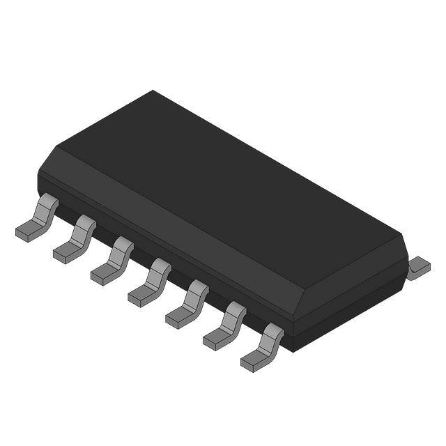
封装信息: - 提供14引脚塑料DIP封装和14引脚窄SOIC封装。 - 封装尺寸和标记信息详细列出,包括英寸和毫米尺寸、最小和最大值。
RC4136M 价格&库存

很抱歉,暂时无法提供与“RC4136M”相匹配的价格&库存,您可以联系我们找货

免费人工找货