RMPA2453

RMPA2453

  • 厂商:

    FAIRCHILD(仙童半导体)

  • 封装:

  • 描述:

    RMPA2453 - 2.4-2.5 GHz InGaP HBT Linear Power Amplifier - Fairchild Semiconductor

  • 详情介绍
  • 数据手册
  • 价格&库存
RMPA2453 数据手册
RMPA2453 July 2004 RMPA2453 2.4–2.5 GHz InGaP HBT Linear Power Amplifier General Description The RMPA2453 power amplifier is designed for high performance WLAN applications in the 2.4–2.5 GHz frequency band. The low profile 16 pin 3 x 3 x 0.9 mm package with internal matching on both input and output to 50Ω minimizes next level PCB space and allows for simplified integration. The on-chip detector provides power sensing capability while the logic control provides power saving shutdown options. The PA’s low power consumption and excellent linearity are achieved using our InGaP Heterojunction Bipolar Transistor (HBT) technology. Features • • • • • • • • • • 26dB small signal gain 26.5dBm output power @ 1dB compression 2.5% EVM at 18dBm modulated output power 3.5% EVM at 19dBm modulated output power 3.3V single positive supply operation Two power saving shutdown options (bias and logic control) Integrated power detector with 20dB dynamic range Low profile 16 pin 3 x 3 x 0.9 mm leadless package Internally matched to 50Ω and DC blocked RF input/ output Optimized for use in 802.11b/g applications Device Functional Block Diagram VDET REF VDET VM12 VC2 16 15 14 13 VL 1 BIAS VOLTAGE DETECTOR 12 N/C RF IN 2 INPUT MATCH INT STG MATCH OUTPUT MATCH 11 RF OUT RF IN 3 10 RF OUT N/C 4 9 N/C 5 6 7 8 Pin 1 2 3 4 5 6 7 8 9 10 11 12 13 14 15 16 Description VL (logic) RF IN RF IN N/C VC1 N/C N/C N/C N/C RF OUT RF OUT N/C VC2 VDET VDET REF VM12 VC1 N/C N/C N/C Backside Ground ©2004 Fairchild Semiconductor Corporation RMPA2453 Rev. D RMPA2453 Absolute Ratings1 Symbol VC1, VC2 IC1, IC2 Parameter Positive Supply Voltage Supply Current IC1 IC2 Positive Bias Voltage Logic Voltage RF Input Power Case Operating Temperature Storage Temperature Ratings 5 120 700 4.0 5 10 -40 to +85 -55 to +150 Units V mA mA V V dBm °C °C VM12 VL PIN TCASE TSTG Notes: 1: No permanent damage with only one parameter set at extreme limit. Other parameters set to typical values Electrical Characteristics1, 3 802.11g OFDM Modulation (RF framed with 176ms burst time 100ms idle time) 54Mbps Data Rate 16.7MHz Bandwidth Parameter Frequency Supply Voltage Gain Total Current @ 18dBm POUT Total Current @ 19dBm POUT EVM @ 18dBm POUT2 EVM @ 19dBm POUT2 Detector Output @ 19dBm POUT Detector Threshold4 POUT Spectral Mask Compliance5 Min 2.4 3.0 24.5 Typ 3.3 26 133 145 2.5 3.5 515 5.0 21.0 Max 2.5 3.6 29 160 165 3.53 4.53 600 7.0 Units GHz V dB mA mA % % mV dBm dBm Electrical Characteristics3, 6 802.11b CCK Modulation (RF not framed) 11Mbps Data Rate 22.0MHz Bandwidth Parameter Frequency Supply Voltage Gain Total Current First Sidelobe Power Second Sidelobe Power Max POUT Spectral Mask Compliance7 Min 2.4 3.0 24.5 Typ 3.3 26 250 -35 -55 24.0 Max 2.5 3.6 29 Units GHz V dB mA dBc dBc dBm Notes: 1: VC1,VC2, VM12 = 3.3V, TC = 25°C, PA is constantly biased, 50Ω system. 2: Percentage includes system noise floor of EVM = 0.8%. 3: EVM not measured 100% in production. 4: POUT measured at PIN corresponding to power detection threshold. 5: Measured at PIN at which Spectral Mask Compliance is satisfied. Two-sample windowing length applied. 6: VC1,VC2, VM12 = 3.3V, TC = 25°C, POUT = +23dBm, 50Ω system. Satisfies spectral mask. 7: PIN is adjusted to point where spectral performance reaches maximum limit. ©2004 Fairchild Semiconductor Corporation RMPA2453 Rev. D RMPA2453 Electrical Characteristics1 Single Tone Parameter Frequency Supply Voltage Gain Total Quiescent Current Bias Current at pin VM122 P1dB Compression Standby Current3 Shutdown Current (VM12 = 0V) Input Return Loss Output Return Loss Detector Output at P1dB Comp Detector POUT Threshold 2nd Harmonic Output at P1dB 3rd Harmonic Output at P1dB Logic Shutdown Control (VL): Device Off, Logic High Input Device On, Logic Low Input Logic Current Turn-on Time4 Turn-off Time Spurious (Stability)5 Notes: 1: VC1,VC2, VM12 = 3.3V, TC = 25°C, 50Ω system. 2: Bias current is included in the Total Quiescent Current. 3: VL is set to Input Logic Level High for PA Off operation. 4: Measured from Device On signal turn on (Logic Low) to the point where RF POUT stabilizes to 0.5dB. 5: Load VSWR is set to 8:1 and the angle is varied 360 degrees. POUT = -30dBm to P1dB. Min 2.4 3.0 24.5 10.0 25 Typ 3.3 26 105 12.5 26.5 0.7
RMPA2453
1. 物料型号: - 型号为RMPA2453,是2.4–2.5 GHz InGaP HBT Linear Power Amplifier。

2. 器件简介: - 
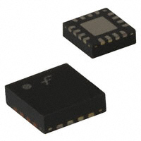
RMPA2453功率放大器针对2.4–2.5 GHz频段的高性能无线局域网(WLAN)应用而设计。该放大器采用16引脚的小型封装,内部匹配至50Ω,以最小化PCB空间并简化集成。它使用InGaP异质结双极晶体管(HBT)技术,实现了低功耗和优异的线性特性。

3. 引脚分配: - 1: VL(logic) - 2: RF IN - 3: RF IN - 4: N/C - 5: VC1 - 6: N/C - 7: N/C - 8: N/C - 9: N/C - 10: RF OUT - 11: RF OUT - 12: N/C - 13: VC2 - 14: VDET - 15: VDET REF - 16: VM12

4. 参数特性: - 26dB小信号增益 - 26.5dBm输出功率@1dB压缩 - 2.5% EVM@18dBm调制输出功率 - 3.5% EVM@19dBm调制输出功率 - 3.3V单正供电操作 - 两种省电关闭选项(偏置和逻辑控制) - 集成20dB动态范围的功率检测器 - 优化用于802.11b/g应用

5. 功能详解: - RMPA2453具有功率检测能力和逻辑控制以节省电源。它通过InGaP HBT技术实现低功耗和优秀的线性特性。

6. 应用信息: - 设计用于802.11b/g应用,需要遵循ESD预防措施以防止静电损伤。

7. 封装信息: - 采用低轮廓16引脚3 x 3 x 0.9 mm无引线封装,内部匹配至50Ω并DC阻断RF输入/输出。
RMPA2453 价格&库存

很抱歉,暂时无法提供与“RMPA2453”相匹配的价格&库存,您可以联系我们找货

免费人工找货