USB1T11A — Universal Serial Bus Transceiver
March 2008
USB1T11A — Universal Serial Bus Transceiver
Features
Complies with Universal Serial Bus Specification 1.1 Utilizes Digital Inputs and Outputs to Transmit and Receive USB Cable Data Supports 12Mbit/s “Full Speed” and 1.5Mbit/s “Low Speed” Serial Data Transmission Compatible with the VHDL “Serial Interface Engine” from USB Implementers' Forum Supports Single-ended Data Interface Single 3.3V Supply ESD Performance: Human Body Model >9.5kV on D-, D+ pins only >4kV on all other pins 16-lead, Space-Saving, MLP Package
Description
The USB1T11A is a one-chip, generic USB transceiver. It is designed to allow 5.0V or 3.3V programmable and standard logic to interface with the physical layer of the Universal Serial Bus. It is capable of transmitting and receiving serial data at both full-speed (12Mbit/s) and low-speed (1.5Mbit/s) data rates. The input and output signals of the USB1T11A conform with the “Serial Interface Engine.” Implementation of the serial interface engine allows designers to make USBcompatible devices with off-the-shelf logic to modify and update the application.
Ordering Information
Part Number
USB1T11AM USB1T11AMX USB1T11ABQX USB1T11AMTC USB1T11AMTCX
Operating Temperature Range
-40 to +85°C -40 to +85°C -40 to +85°C -40 to +85°C -40 to +85°C
Package
14-Lead, Small Outline Integrated Circuit (SOIC), JEDEC MS-012, 0.150-Inch Narrow 14-Lead, Small Outline Integrated Circuit (SOIC), JEDEC MS-012, 0.150-Inch Narrow 16-Terminal, Molded Leadless Package (MLP), JEDEC MO-220, 3mm Square 14-Lead, Thin Shrink Small Outline Package (TSSOP), JEDEC MO-153, 4.4mmWide 14-Lead, Thin Shrink Small Outline Package (TSSOP), JEDEC MO-153, 4.4mm Wide
Packing Method
Tube Tape and Reel Tape and Reel Tube Tape and Reel
All packages are lead free per JEDEC: J-STD-020B standard.
/OE SPEED VMO/FSE0
DD+
+ -
VPO
RCV
VP
VM
Figure 1. Logic Diagram
© 1999 Fairchild Semiconductor Corporation USB1T11A • Rev. 1.0.2 www.fairchildsemi.com
�USB1T11A — Universal Serial Bus Transceiver
Pin Configuration
Speed D-
14
/OE
2
13
VMO/FSEO
12 VPO 13 14 15
D+
MODE
1
VCC
11
10
NC
9 8 7 6
NC
RCV
3
12
VPO
NC GND
VP VM SUSPND
4
11
D+
VMO/FSEO SUSPND
5
10
DVCC
16 1
Mode
5 2
/OE
VM
6
9
SPEED
3
RCV
4
VP
GND
7
8
NC
Figure 2. TSSOP and SOIC Pin Assignments
Figure 3. MLP Pin Assignments
Pin Descriptions
Pin Names
RVC /OE Mode
I/O
O I I
Description
Receive Data. CMOS level output for USB differential input. Output Enable. Active LOW, enables the transceiver to transmit data on the bus. When not active, the transceiver is in receive mode. Mode. When left unconnected, a weak pull-up transistor pulls it to VCC and, in this GND, the VMO/FSEO pin takes the function of FSEO (force SEO). Inputs to differential driver. (Outputs from SIE.)
Mode
0
VPO
0 0 1 1
VMO/FSEO
RESULT
Logic “0” /SEO Logic “1” /SEO
VPO,VMO/FSEO
I 1
0 0 1 1
0 1 0 1
/SEO Logic “0” Logic “1” Illegal Code
Gated version of D- and D+. Outputs are logic “0” and logic “1.” Used to detect single ended zero (/SEO), error conditions, and interconnected speed. (Input to SIE).
VP
VP,VM O 0 0 1 0 D+, DSUSPND Speed VCC GND
© 1999 Fairchild Semiconductor Corporation USB1T11A • Rev. 1.0.2
VM
0 1 0 1
RESULT
/SEO Low Speed Full Speed Error
AI/O I I
Data+, Data-. Differential data bus conforming to the Universal Serial Bus standard. Suspend. Enables a low-power state while the USB bus is inactive. While the suspend pin is active, it drives the RCV pin to a logic “0” state. Both D+ and D- are 3STATE. Edge Rate Control. Logic “1” operates at edge rates for “full speed.” Logic “0” operates edge rates for “low speed.” 3.0 to 3.6 power supply. Ground reference.
www.fairchildsemi.com 2
�USB1T11A — Universal Serial Bus Transceiver
Functional Truth Table
Input
Mode
0 0 0 0 1 1 1 1 Don’t Care Don’t Care
I/O
/OE
0 0 0 0 0 0 0 0 1 1
Outputs
D1 0 0 0 0 1 0 1
VPO
0 0 1 1 0 0 1 1 Don’t Care Don’t Care
VMO/FSEO
0 1 0 1 0 1 0 1 Don’t Care Don’t Care
SUSPND
0 0 0 0 0 0 0 0 0 1
D+
0 0 1 0 0 0 1 1 3-State 3-State
RCV
0 Undefined State 1 Undefined State Undefined State 0 1 Undefined State Undefined State Undefined State
VP
0 0 1 0 0 0 1 Undefined State Undefined State Undefined State
VM
1 0 0 0 0 1 0 Undefined State Undefined State Undefined State
Result
Logic “0” /SEO Logic “1” /SEO /SEO Logic “0” Logic “1” Illegal Code D+/DHi-Z D+/DHi-Z
3-State 3-State
© 1999 Fairchild Semiconductor Corporation USB1T11A • Rev. 1.0.2
www.fairchildsemi.com 3
�USB1T11A — Universal Serial Bus Transceiver
Absolute Maximum Ratings
Stresses exceeding the absolute maximum ratings may damage the device. The device may not function or be operable above the recommended operating conditions and stressing the parts to these levels is not recommended. In addition, extended exposure to stresses above the recommended operating conditions may affect device reliability. The absolute maximum ratings are stress ratings only.
Symbol
VCC IIK VIN VI/O IOK VO IO ICC / IGND TSTG DC Supply Voltage
Parameter
DC Input Diode Current, VINVCC or VO
很抱歉,暂时无法提供与“USB1T11AMX”相匹配的价格&库存,您可以联系我们找货
免费人工找货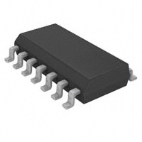


 工商网监
湘ICP备2023018690号
工商网监
湘ICP备2023018690号