Formosa MS
N-Channel SMD MOSFET ESD Protection
2N7002K
List
List................................................................................................. 1
Package outline............................................................................... 2
Features.......................................................................................... 2
Mechanical data............................................................................... 2
Maximum ratings ............................................................................. 2~3
Rating and characteristic curves........................................................ 4~5
Pinning information........................................................................... 6
Marking........................................................................................... 6
Suggested solder pad layout............................................................. 6
Packing information.......................................................................... 7
Reel packing.................................................................................... 8
Suggested thermal profiles for soldering processes............................. 8
High reliability test capabilities........................................................... 9
http://www.formosams.com/
TEL:886-2-22696661
FAX:886-2-22696141
Page 1
Document ID
Issued Date
Revised Date
DS-251105
2008/02/10
2012/10/24
Revision
G
Page.
9
�Formosa MS
N-Channel SMD MOSFET ESD Protection
2N7002K
60V N-Channel Enhancement
Mode MOSFET- ESD Protection
Features
Package outline
• R DS(ON), V GS@10V, I D@500mA=3.0 Ω
• R DS(ON), V GS@4.5V, I D@200mA=4.0 Ω
• ESD protection 2ΚV (Human body mode)
• Advanced trench process technology.
• High density cell design for ultra low on-resistance.
• Very low leakage current in off condition
• Specially designed for battery operated system,
(B)
0.012 (0.30)
0.020 (0.50)
0.034 (0.85)
0.045 (1.15)
.084(2.10)
.068(1.70)
0.110 (2.80)
solid-state relays drivers, relays, displays, lamps,
solenoids, memories, etc.
In compliance with EU RoHS 2002/95/EC directives.
Suffix "-H" indicates Halogen-free part, ex. 2N7002K-H.
0.120 (3.04)
(C)
(A)
0.063 (1.60)
0.027 (0.67)
0.013 (0.32)
0.047 (1.20)
0.108 (2.75)
Mechanical data
0.007 (0.18)
0.083 (2.10)
• Epoxy:UL94-V0 rated flame retardant
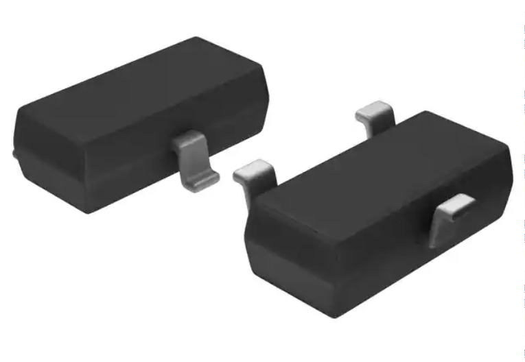
• Case : Molded plastic, SOT-23
• Terminals : Solder plated, solderable per
0.051 (1.30)
0.003 (0.09)
•
•
SOT-23
0.035 (0.89)
MIL-STD-750, Method 2026
• Mounting Position : Any
• Weight : Approximated 0.008 gram
M aximum ratings (AT T
A
Dimensions in inches and (millimeters)
=25 oC unless otherwise noted)
PARAMETER
Symbol
Ratings
UNIT
Drain-Source voltage
V DS
60
V
Gate-source voltage
V GS
±20
V
Continuous drain current
ID
300
mA
I DM
2000
mA
Pulsed drain current
1)
PARAMETER
Symbol
P D@T A= 25°C
Total power dissipation
MIN.
TYP.
Thermal resistance(PCB mounted)
2)
W
0.21
T J , T STG
Junction to ambient
UNIT
0.35
PD
P D@ T A=75°C
Operation junction and storage temperature range
MAX.
o
357
R θJA
o
+150
-55
C
C/W
Note : 1. Maximum DC current limited by package
2. Surface mounted on FR4 board, t < 5 sec
http://www.formosams.com/
TEL:886-2-22696661
FAX:886-2-22696141
Page 2
Document ID
Issued Date
Revised Date
DS-251105
2008/02/10
2012/10/24
Revision
G
Page.
9
�Formosa MS
N-Channel SMD MOSFET ESD Protection
2N7002K
Electrical characteristics (AT T =25 C unless otherwise noted)
o
A
STATIC
PARAMETER
CONDITIONS
Drain-source Breakdown Voltage
Gate Threshold Voltage
Symbol
MIN.
V GS = 0V, I D = 10µA
BV DSS
60
V DS = V GS , I D = 250µA
V GS(th)
1.0
TYP.
MAX.
UNIT
V
2.5
V GS = 10V, I D = 500mA
V
3.0
Drain-Source On-State Resistance
Ω
R DS(on)
V GS = 4.5V, I D = 200mA
4.0
V DS = 60V, V GS = 0V
I DSS
1
µA
Gate-Body leakage Current
V GS = ±20V, V DS = 0V
I GSS
±10
µA
Forward TransConductance
V DS = 15V, I D = 250mA
g fS
V DS = 15V, I D = 200mA
V GS = 4.5V
Qg
0.8
t on
20
t off
40
Zero Gate Voltage Drai n Current
ms
100
DYNAMIC
Total Gate Charge
Turn-On Delay Time
V DD = 30V, R L = 150Ω, I D = 200mA,
V gen = 10V, R G = 10Ω
Turn-Off Delay Time
ns
Input Capacitance
V DS = 25V, V GS = 0V
f = 1.0 MHz
Output Capacitance
nC
Reverse Transfer Capacitance
C iss
35
C oss
10
C rss
5
pF
Source-Drain Diode
Diode Forward Voltage
V SD
I S=200mA, V GS=0V
Switching
Test Circuit
0.82
Gate Charge
Test Circuit
V DD
V DD
RL
V IN
V GS
V
1.3
RL
V OUT
D
V GS
D
1mA
RG
V GS
DUT
DUT
G
G
RG
S
http://www.formosams.com/
TEL:886-2-22696661
FAX:886-2-22696141
S
Page 3
Document ID
Issued Date
Revised Date
DS-251105
2008/02/10
2012/10/24
Revision
G
Page.
9
�Rating and characteristic curves (2N7002K)
Fig.2 Transfer Characteristic
V GS = 6.0~10V
I D - Drain Source Current (A)
I D - Drain-to-Source Current (A)
Fig.1 Output Characteristic
5.0V
4.0V
3.0V
V DS = 10V
V GS - Gate-to-Source Voltage (V)
V DS - Drain-to-Source Voltage (V)
Fig.4 On Resistance vs Gate to Source Voltage
Fig.3 On Resistance vs Drain Current
R DS(ON) - On-Resistance(Ω)
R DS(ON) - On-Resistance(Ω)
5
4
3
V GS = 4.5V
2
1
V GS = 10V
5
4
3
I D = 500mA
2
I D = 200mA
1
0
0
0
0.2
0.4
0.6
0.8
1.0
1.2
2
3
4
5
6
7
8
9
10
V GS - Gate-to-Source Voltage (V)
I D - Drain Current (A)
RDS(ON) - On-Resistance(Normalized)
Fig.5 On Resistance vs Junction Temperature
V GS = 10V
I D = 500mA
T J - Junction Temperature (°C)
http://www.formosams.com/
TEL:886-2-22696661
FAX:886-2-22696141
Page 4
Document ID
Issued Date
Revised Date
DS-251105
2008/02/10
2012/10/24
Revision
G
Page.
9
�Rating and characteristic curves (2N7002K)
Fig.7 Gate Charge
V GS - Gate-to-Source Voltage (V)
Fig. 6 Gate Charge Waveform
Vgs
Qg
Qsw
Vgs(th)
10
V DS = 10V
8
I D = 250mA
6
4
2
0
0
Qg(th)
Qgs
0.4
0.6
0.8
1.0
Qg - Gate Charge (nC)
Qg
Qgd
Fig.9 Breakdown Voltage vs Junction Temperature
Fig.8 Threshold Voltage vs Temperature
V th - G-S Threshold Voltage (NORMALIZED)
0.2
BV DSS -Breakdown Voltage (V)
90
I D = 250uA
I D = 250uA
88
86
84
82
80
78
76
74
72
-50
T J - Junction Temperature (°C)
-25
0
25
50
75
100
125
150
T J - Junction Temperature (°C)
Fig.10 Source-Drain Diode Forward Voltage
10
I S - Source Current (A)
V GS = 0V
o
25 C
1
o
125 C
o
-55 C
0.1
0.01
0.2
0.4
0.6
0.8
1.0
1.2
1.4
1.6
1.8
V SD - Source-to-Drain Voltage (V)
http://www.formosams.com/
TEL:886-2-22696661
FAX:886-2-22696141
Page 5
Document ID
Issued Date
Revised Date
DS-251105
2008/02/10
2012/10/24
Revision
G
Page.
9
�Formosa MS
N-Channel SMD MOSFET ESD Protection
2N7002K
Pinning information
Pin
Simplified outline
Symbol
D
PinD
PinG
PinS
Drain
Drain
Gate
Source
Gate
G
Source
S
Marking
Type number
Marking code
RK
M
K72
2N7002K
M
02KYM
(Note 1)
(Note 2)
(Note 2)
Note:1.YM indicate Date ode, indicate Halogen-Free.
Y= year code, 8=2008, 9=2009
M= week code, A~Z = 1st ~ 26th week
a ~z= 27th ~ 52nd week
. =53rd week
2.M = Month code
Suggested solder pad layout
SOT-23
0.037(0.95)
0.037(0.95)
0.079(2.0)
0.035(0.90)
0.031(0.80)
Dimensions in inches and (millimeters)
http://www.formosams.com/
TEL:886-2-22696661
FAX:886-2-22696141
Page 6
Document ID
Issued Date
Revised Date
DS-251105
2008/02/10
2012/10/24
Revision
G
Page.
9
�Formosa MS
N-Channel SMD MOSFET ESD Protection
2N7002K
Packing information
P0
P1
d
E
F
B
A
W
P
D2
D1
T
C
W1
D
unit:mm
Item
Symbol
Tolerance
SOT-23
Carrier width
Carrier length
Carrier depth
Sprocket hole
13" Reel outside diameter
13" Reel inner diameter
7" Reel outside diameter
7" Reel inner diameter
Feed hole diameter
Sprocket hole position
Punch hole position
Punch hole pitch
Sprocket hole pitch
Embossment center
Overall tape thickness
Tape width
Reel width
A
B
C
d
D
D1
D
D1
D2
E
F
P
P0
P1
T
W
W1
0.1
0.1
0.1
0.1
2.0
min
2.0
min
0.5
0.1
0.1
0.1
0.1
0.1
0.1
0.3
1.0
3.15
2.77
1.22
1.50
178.00
55.00
13.00
1.75
3.50
4.00
4.00
2.00
0.23
8.00
12.0
Note:Devices are packed in accor dance with EIA standar RS-481-A and specifications listed above.
http://www.formosams.com/
TEL:886-2-22696661
FAX:886-2-22696141
Page 7
Document ID
Issued Date
Revised Date
DS-251105
2008/02/10
2012/10/24
Revision
G
Page.
9
�Formosa MS
N-Channel SMD MOSFET ESD Protection
2N7002K
Reel packing
PACKAGE
REEL SIZE
SOT-23
7"
REEL
(pcs)
COMPONENT
SPACING
(m/m)
BOX
(pcs)
INNER
BOX
(m/m)
REEL
DIA,
(m/m)
3,000
4.0
15,000
183*183*123
178
CARTON
SIZE
(m/m)
382*262*387
CARTON
(pcs)
APPROX.
GROSS WEIGHT
(kg)
11.6
240,000
Suggested thermal profiles for soldering processes
1.Storage environment: Temperature=5 oC ~40 oC Humidity=55%±25%
2.Reflow soldering of surface-mount devices
Critical Zone
TL to TP
Tp
TP
Ramp-up
TL
TL
Tsmax
Temperature
Tsmin
tS
Preheat
Ramp-down
25
t25o C to Peak
Time
3.Reflow soldering
Profile Feature
Soldering Condition
Average ramp-up rate(T L to T P )
o
很抱歉,暂时无法提供与“2N7002K”相匹配的价格&库存,您可以联系我们找货
免费人工找货