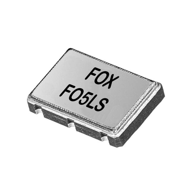
FO5LS
5.0mm x 3.2mm
SMD LVDS Oscillator
(Former F530D/F540D families)
Features
•
•
•
•
LVDS Output
Stabilities to ±20 PPM
Operating Temperature Ranges to -40°C to +85°C
Supply Voltages: 1.8V, 2.5V, 3.3V
2.5/3.3V SPECIFICATIONS
PARAMETERS
Frequency Range
Temperature Range
Storage (TSTG)
Supply Voltage (VDD)
Input Current
(IDD)
Standby Current
Output Symmetry (50% VP-P)
Rise Time (20%~80% VP-P)
Fall Time (80%~20% VP-P)
Differential Output Voltage (VOD)
Differential Offset Voltage (VOS)
Differential Output Voltage Swing (Vopp)
Output Load
(HCMOS)
Start-up Time
(TS)
Output Disable Time 1
Output Enable Time 1
Aging (per year @ 25C)
Phase Jitter (12kHz~20MHz)
MAX (Unless otherwise noted)
13.5 ~ 250MHz
-55°C ~ +125°C
2.5V±10%
50 mA
15 µA
45 % ~ 55 %
0.5 nS
0.5 nS
0.247V ~ 0.454V
1.125V ~ 1.375V
0.25Vpp min
100 Ohms Typical
10 mS
200 µS
10 mS
±3 PPM
1 pS
3.3V±10%
0.35Vpp min
ENABLE / DISABLE FUNCTION
Pin1
OPEN 1
‘1’ Level VIH ≥ 70%VDD
‘0’ Level VIL ≤ 30%VDD
Out 1 (pin 4), Out 2 (pin 5)
Active
Active
High Z
Available Options by Stability & Operating Temp
Frequency Stability2
±100PPM
±100PPM
±100PPM
±50PPM
±50PPM
±50PPM
±25PPM
±25PPM
±25PPM3
±20PPM3
Revised A: 05/06/2020
Operating Temperature (°C)
-10 ~ +70
-20 ~ +70
-40 ~ +85
-10 ~ +70
-20 ~ +70
-40 ~ +70
-10 ~ +85
-20 ~ +70
-40 ~ +85
-20 ~ +70
Frequency Range (MHz)
13.500 ~ 250.000
13.500 ~ 250.000
13.500 ~ 250.000
13.500 ~ 250.000
13.500 ~ 250.000
13.500 ~ 250.000
13.500 ~ 250.000
13.500 ~ 250.000
13.500 ~ 250.000
13.500 ~ 250.000
Page 1 of 4
www.foxonline.com
�FO5LS
5.0mm x 3.2mm
SMD LVDS Oscillator
(Former F530D/F540D families)
1.8V SPECIFICATIONS
PARAMETERS
Frequency Range
Temperature Range
Storage (TSTG)
Supply Voltage (VDD)
Input Current
(IDD)
Standby Current
Output Symmetry (50% Vp-p)
Rise Time (20%~80% VP-P)
Fall Time (80%~20% VP-P)
Differential Output Voltage (VOD)
Differential Offset Voltage (VOS)
Differential Output Voltage Swing (Vopp)
Output Load
(HCMOS)
Start-up Time
(TS)
Output Disable Time 1
Output Enable Time 1
Aging (per year @ 25C)
Phase Jitter (12kHz~20MHz)
MAX (Unless otherwise noted)
100 ~ 170MHz
-55°C ~ +125°C
1.8V±10%
66 mA
30 µA
45% ~ 55%
0.7 nS
0.7 nS
0.33V typ
1.125V ~ 1.375V (1.25V typ)
0.25Vp-p min
100 Ohms Typical
10 mS
200 nS
10 mS
±3 PPM
1 pS (0.5pS typ)
ENABLE / DISABLE FUNCTION
Pin1
OPEN 1
‘1’ Level VIH ≥ 70%VDD
‘0’ Level VIL ≤ 30%VDD
Out 1 (pin 4), Out 2 (pin 5)
Active
Active
High Z
Available Options by Stability & Operating Temp
Frequency Stability2
±100PPM
±100PPM
±50PPM
±50PPM
±25PPM
±25PPM3
Operating Temperature (°C)
-20 ~ +70
-40 ~ +85
-20 ~ +70
-40 ~ +85
-20 ~ +70
-40 ~ +85
Frequency Range (MHz)
100.0 ~ 170.0
100.0 ~ 170.0
100.0 ~ 170.0
100.0 ~ 170.0
100.0 ~ 170.0
100.0 ~ 170.0
An internal pull-up resistor from pin 1 to pin 6 allows active output if pin 1 is left open
Inclusive of 25°C tolerance, operating temperature range, input voltage change, load change,
Reflow, one-year aging, shock, and vibration.
3 Inclusive of 25°C tolerance and operating temperature range.
1
2
Revised A: 05/06/2020
Page 2 of 4
www.foxonline.com
�FO5LS
5.0mm x 3.2mm
SMD LVDS Oscillator
(Former F530D/F540D families)
DIMENSIONS / MECHANICAL
SPECIFICATIONS
`
Note:
1. A 0.01μF capacitor should be placed between VDD
(Pin 6) and GND (Pin3) to minimize power supply line
noise.
2. Dimensional drawing is for reference to critical
specifications defined by size measurements. Certain
non-critical visual attributes, such as side castellation’s,
pin shape etc. may vary.
STANDARD SPECIFICATIONS
PARAMETERS
Maximum Soldering Temp / Time
Moisture Sensitivity Level (MSL)
Termination Finish
Seal Method
Lead (Pb) Free
REACH/REACH Compliant
Revised A: 05/06/2020
MAX (Unless otherwise noted)
260°C / 10 Seconds x 2
1
Au over Ni
Seam
Yes
Yes
Page 3 of 4
www.foxonline.com
�FO5LS
5.0mm x 3.2mm
SMD LVDS Oscillator
(Former F530D/F540D families)
TAPE SPECIFICATIONS (mm)
REEL SPECIFICATIONS (mm)
A
B
C
D
E
F
REEL QTY
G
H
I
J
K
L
M
ø1.5
4.0
480
3.5
16.0
1.4
-T1 = 1,000
2.0
Ø13
Ø21
Ø60
Ø180
13.0
2.0
Available Options & Part Identification for SMD LVDS Oscillator O5LS*
Sample PN: FO5LSCDM125.0 -T1
F
O5LS
C
D
M
125.0
-T1
Fox
Model
Number
Voltage
K = 1.8V±5%
J = 2.5V±10%
C = 3.3V±10%
Stability
A = ±100 PPM
B = ±50 PPM
D = ±25 PPM
E = ±20 PPM
Operating
Temperature
E = -10 to +70°C
F = -20 to +70°C
M = -40 to +85°C
Frequency (MHz)
Reel Quantity
Blank = Bulk
T1 = 1,000 pcs
* Not all frequencies in the frequency range, or every combination of stability, temp range, and voltage available. See stabilities and
op temps for each VDD.
Reliability Test Conditions
Please contact Abracon Quality Assurance department
Revised A: 05/06/2020
Page 4 of 4
www.foxonline.com
�
FO5LSCDM156.25-BULK 价格&库存
很抱歉,暂时无法提供与“FO5LSCDM156.25-BULK”相匹配的价格&库存,您可以联系我们找货
免费人工找货