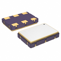
for
ETHERNET
3.3V 50ppm
LVDS 7 x 5mm
Features
Model: FXO-LC735RGB-125 XO Freq: 125MHz
Low Jitter Low Cost Tri-State Enable / Disable Feature Industry Standard Package Gold over Nickel Termination Finish
V DD Enable / Disable
X PRESSO
ASICs
GND
FOX
OUTPUT
Electrical Characteristics
Parameters
Frequency Frequency Stability 1 Temperature Range Supply Voltage Input Current Output Load Start-Up Time Output Enable / Disable Time Moisture Sensitivity Level Termination Finish MSL TO TSTG VDD IDD Differential TS Standard operating Storage Standard Standard Load Standard
Symbol
FO
Condition
Maximum Value
(unless otherwise noted) 125 MHz 50 ppm -40°C to +85°C -55°C to +125°C 3.3V ± 5% 100 mA 100 ohms Typ. 10 mS 100 nS 1 Au
Note 1 – Stability is inclusive of 25°C tolerance, operating temperature range, input voltage change, load change, aging, shock and vibration.
Output Wave Characteristics
Parameters
Differential Output Voltage Output Offset Voltage Output Symmetry Output Enable (PIN # 1) Voltage Output Disable (PIN # 1) Voltage Cycle Rise Time Cycle Fall Time
DWG-100719 | Rev. 6/2/2010
Symbol
VOD VOS VIH VIL TR TF
Condition
Standard Load Standard Load @ 50% Vp-p Level
Maximum Value
0.6V Typ. 1.3V Typ. 45% ~ 55% ≥70% VDD ≤ 30% VDD 400 pS 400 pS
20% ~ 80% Vp-p 80% ~ 20% Vp-p
Page 1 of 2
FOXElectronics 5570 Enterprise Parkway Fort Myers, Florida 33905 USA +1.239.693.0099 FAX +1.239.693.1554 FOXONLINE EMEA Tel/Fax: +44 .1767.312632 | Asia Hong Kong Tel: +852.2854.4285 Fax +852.2854.4282 | Japan Tel: +81.3.3374.2079 Fax: +81.3.3374.5221 © 2010 FOX ELECTRONICS | ISO9001:2000 Certified
�for
ETHERNET
3.3V 50ppm
LVDS 7 x 5mm
Model: FXO-LC735RGB-125 XO Freq: 125MHz
Dimensional Drawing & Pad Layout
Phase Jitter & Time Interval Error (TIE) (Typical Measurements)
Frequency
125 MHz
Phase Jitter
(12kHz to 20MHz)
TIE
(Sigma of Jitter Distribution)
Units
pS RMS
0.77
3.0
Phase Jitter is integrated from HP3048 Phase Noise Measurement System; measured directly into 50 ohm input; VDD = 3.3V. TIE was measured on LeCroy LC684 Digital Storage Scope, directly into 50 ohm input, with Amherst M1 software; VDD = 3.3V.
Per MJSQ spec (Methodologies for Jitter and Signal Quality specifications)
Random & Deterministic Jitter Composition (Typical Measurements)
Frequency
125 MHz
Random (Rj)
(pS RMS)
Deterministic (Dj)
(pS P-P)
Total Jitter (Tj)
(14 x Rj) + Dj 24.9 pS
1.3
7.0
Rj and Dj, measured on LeCroy LC684 Digital Storage Scope, directly into 50 ohm input, with Amherst M1 software.
Per MJSQ spec (Methodologies for Jitter and Signal Quality specifications)
Pin Functional Description
Pin #
1 2 3 4 5 6
Name
E/D
NC 1
Type
Logic Ground Output Output Power
Function
Enable / Disable Control of Output (0 = Disabled)
No Connection – Leave Open
GND Output Output 2 VDD 2
1 2
Electrical Ground for VDD LVDS Oscillator Output Complementary LVDS Output Power Supply Source Voltage
NOTES:
Includes pull-up resistor to VDD to provide output when the pin (1) is No Connect. Installation should include a 0.01µF bypass capacitor placed between VDD (Pin 6) and GND (Pin 3) to minimize power supply line noise.
DWG-100719 | Rev. 6/2/2010
Page 2 of 2
© 2010 FOX ELECTRONICS | ISO9001:2000 Certified | FOXONLINE
�
很抱歉,暂时无法提供与“FXO-LC735RGB-125”相匹配的价格&库存,您可以联系我们找货
免费人工找货