NXP Semiconductors
Data Sheet: Technical Data
MC9S08PL60 Series Data
Sheet
Document Number MC9S08PL60
Rev. 2, 01/2019
MC9S08PL60
Supports: MC9S08PL60 and
MC9S08PL32
Key features
• 8-Bit S08 central processor unit (CPU)
– Up to 20 MHz bus at 2.7 V to 5.5 V across
temperature range of -40 °C to 85 °C
– Supporting up to 40 interrupt/reset sources
– Supporting up to four-level nested interrupt
– On-chip memory
– Up to 60 KB flash read/program/erase over full
operating voltage and temperature
– Up to 256 byte EEPROM; 2-byte erase sector;
program and erase while executing flash
– Up to 4096 byte random-access memory (RAM)
– Flash and RAM access protection
• Power-saving modes
– One low-power stop mode; reduced power wait
mode
– Peripheral clock enable register can disable clocks to
unused modules, reducing currents; allows clocks to
remain enabled to specific peripherals in stop3 mode
• Clocks
– Oscillator (XOSC) - loop-controlled Pierce
oscillator; crystal or ceramic resonator range of
31.25 kHz to 39.0625 kHz or 4 MHz to 20 MHz
– Internal clock source (ICS) - containing a frequencylocked-loop (FLL) controlled by internal or external
reference; precision trimming of internal reference
allowing 1% deviation across temperature range of 0
°C to 70 °C and 2% deviation across temperature
range of -40 °C to 85 °C; up to 20 MHz
• System protection
– Watchdog with independent clock source
– Low-voltage detection with reset or interrupt;
selectable trip points
– Illegal opcode detection with reset
– Illegal address detection with reset
• Development support
– Single-wire background debug interface
– Breakpoint capability to allow three breakpoints
setting during in-circuit debugging
– On-chip in-circuit emulator (ICE) debug module
containing two comparators and nine trigger modes
• Peripherals
– ACMP - one analog comparator with both positive
and negative inputs; separately selectable interrupt
on rising and falling comparator output; filtering
– ADC - 16-channel, 10-bit resolution; 2.5 µs
conversion time; data buffers with optional
watermark; automatic compare function; internal
bandgap reference channel; operation in stop mode;
optional hardware trigger
– CRC - programmable cyclic redundancy check
module
– FTM - three flex timer modulators modules
including one 6-channel and two 2-channel ones;
16-bit counter; each channel can be configured for
input capture, output compare, edge- or centeraligned PWM mode
– MTIM - one modulo timers with 8-bit prescaler and
overflow interrupt
– RTC - 16-bit real timer counter (RTC)
– SCI - three serial communication interface (SCI/
UART) modules optional 13-bit break; full duplex
non-return to zero (NRZ); LIN extension support
• Input/Output
– Up to 57 GPIOs including one output-only pin
– Two 8-bit keyboard interrupt modules (KBI)
– Two true open-drain output pins
• Package options
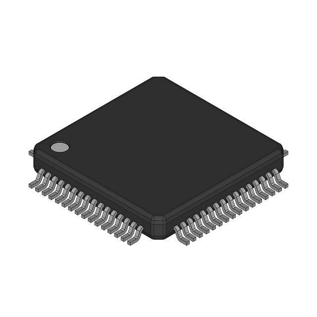
– 64-pin QFP
– 44-pin LQFP
– 32-pin LQFP
NXP reserves the right to change the production detail specifications as may be
required to permit improvements in the design of its products.
�Table of Contents
1 Ordering information............................................................................3
5.2.1
Control timing................................................................ 13
2 Part identification................................................................................. 3
5.2.2
Debug trace timing specifications..................................14
2.1 Description...................................................................................3
5.2.3
FTM module timing....................................................... 15
2.2 Format.......................................................................................... 3
5.3 Thermal specifications................................................................. 16
2.3 Fields............................................................................................4
5.3.1
Thermal operating requirements.................................... 16
2.4 Example....................................................................................... 4
5.3.2
Thermal characteristics.................................................. 16
3 Parameter Classification.......................................................................4
6 Peripheral operating requirements and behaviors................................ 17
4 Ratings..................................................................................................5
6.1 External oscillator (XOSC) and ICS characteristics....................17
4.1 Thermal handling ratings............................................................. 5
6.2 NVM specifications..................................................................... 19
4.2 Moisture handling ratings............................................................ 5
6.3 Analog..........................................................................................20
4.3 ESD handling ratings................................................................... 5
6.3.1
ADC characteristics....................................................... 20
4.4 Voltage and current operating ratings..........................................6
6.3.2
Analog comparator (ACMP) electricals.........................23
5 General................................................................................................. 7
7 Dimensions...........................................................................................23
5.1 Nonswitching electrical specifications........................................ 7
7.1 Obtaining package dimensions.................................................... 23
5.1.1
DC characteristics.......................................................... 7
8 Pinout................................................................................................... 24
5.1.2
Supply current characteristics........................................ 11
8.1 Signal multiplexing and pin assignments.................................... 24
5.1.3
EMC performance..........................................................12
8.2 Device pin assignment................................................................. 26
5.2 Switching specifications.............................................................. 13
9 Revision history....................................................................................29
MC9S08PL60 Series Data Sheet, Rev. 2, 01/2019
2
NXP Semiconductors
�Ordering information
1 Ordering information
The following table summarizes the part numbers of the devices covered by this
document.
Table 1. Ordering information
Feature
MC9S08PL60
Part Number
MC9S08PL32
CQH
CLD
CLC
CQH
CLD
CLC
Max. frequency
(MHz)
20
20
20
20
20
20
Flash memory
(KB)
60
60
60
32
32
32
RAM (KB)
4
4
4
4
4
4
EEPROM (B)
256
256
256
256
256
256
10-bit ADC
16ch
12ch
12ch
16ch
12ch
12ch
1
1
1
1
1
1
6ch+2ch+2ch
6ch+2ch+2ch
6ch+2ch+2ch
6ch+2ch+2ch
6ch+2ch+2ch
6ch+2ch+2ch
1
1
1
1
1
1
Yes
Yes
Yes
Yes
Yes
Yes
SCI (LIN
Capable)
3
3
3
3
3
3
Watchdog
Yes
Yes
Yes
Yes
Yes
Yes
CRC
Yes
Yes
Yes
Yes
Yes
Yes
KBI pins
16
16
13
16
16
13
GPIO
57
42
30
57
42
30
64-QFP
44-LQFP
32-LQFP
64-QFP
44-LQFP
32-LQFP
ACMP
16-bit FlexTimer
8-bit Modulo
timer
RTC
Package
2 Part identification
2.1 Description
Part numbers for the chip have fields that identify the specific part. You can use the
values of these fields to determine the specific part you have received.
2.2 Format
Part numbers for this device have the following format:
MC9S08PL60 Series Data Sheet, Rev. 2, 01/2019
NXP Semiconductors
3
�Parameter Classification
MC 9 S08 PL AA B CC
2.3 Fields
This table lists the possible values for each field in the part number (not all combinations
are valid):
Field
Description
Values
MC
Qualification status
• MC = fully qualified, general market flow
9
Memory
• 9 = flash based
S08
Core
• S08 = 8-bit CPU
PL
Device family
• PL
AA
Approximate flash size in KB
• 60 = 60 KB
• 32 = 32 KB
B
Operating temperature range (°C)
• C = –40 to 85
CC
Package designator
• QH = 64-pin QFP
• LD = 44-pin LQFP
• LC = 32-pin LQFP
2.4 Example
This is an example part number:
MC9S08PL60CQH
3 Parameter Classification
The electrical parameters shown in this supplement are guaranteed by various methods.
To give the customer a better understanding, the following classification is used and the
parameters are tagged accordingly in the tables where appropriate:
Table 2. Parameter Classifications
P
Those parameters are guaranteed during production testing on each individual device.
C
Those parameters are achieved by the design characterization by measuring a statistically relevant sample size
across process variations.
T
Those parameters are achieved by design characterization on a small sample size from typical devices under
typical conditions unless otherwise noted. All values shown in the typical column are within this category.
D
Those parameters are derived mainly from simulations.
MC9S08PL60 Series Data Sheet, Rev. 2, 01/2019
4
NXP Semiconductors
�Ratings
NOTE
The classification is shown in the column labeled “C” in the
parameter tables where appropriate.
4 Ratings
4.1 Thermal handling ratings
Symbol
Description
Min.
Max.
Unit
Notes
TSTG
Storage temperature
–55
150
°C
1
TSDR
Solder temperature, lead-free
—
260
°C
2
1. Determined according to JEDEC Standard JESD22-A103, High Temperature Storage Life.
2. Determined according to IPC/JEDEC Standard J-STD-020, Moisture/Reflow Sensitivity Classification for Nonhermetic
Solid State Surface Mount Devices.
4.2 Moisture handling ratings
Symbol
MSL
Description
Moisture sensitivity level
Min.
Max.
Unit
Notes
—
3
—
1
1. Determined according to IPC/JEDEC Standard J-STD-020, Moisture/Reflow Sensitivity Classification for Nonhermetic
Solid State Surface Mount Devices.
4.3 ESD handling ratings
Symbol
Description
Min.
Max.
Unit
Notes
VHBM
Electrostatic discharge voltage, human body model
-6000
+6000
V
1
VCDM
Electrostatic discharge voltage, charged-device model
-500
+500
V
2
Latch-up current at ambient temperature of 85
-100
+100
mA
ILAT
1. Determined according to JEDEC Standard JESD22-A114, Electrostatic Discharge (ESD) Sensitivity Testing Human Body
Model (HBM).
2. Determined according to JEDEC Standard JESD22-C101, Field-Induced Charged-Device Model Test Method for
Electrostatic-Discharge-Withstand Thresholds of Microelectronic Components.
MC9S08PL60 Series Data Sheet, Rev. 2, 01/2019
NXP Semiconductors
5
�Ratings
4.4 Voltage and current operating ratings
Absolute maximum ratings are stress ratings only, and functional operation at the
maxima is not guaranteed. Stress beyond the limits specified in below table may affect
device reliability or cause permanent damage to the device. For functional operating
conditions, refer to the remaining tables in this document.
This device contains circuitry protecting against damage due to high static voltage or
electrical fields; however, it is advised that normal precautions be taken to avoid
application of any voltages higher than maximum-rated voltages to this high-impedance
circuit. Reliability of operation is enhanced if unused inputs are tied to an appropriate
logic voltage level (for instance, either VSS or VDD) or the programmable pullup resistor
associated with the pin is enabled.
Symbol
Description
Min.
Max.
Unit
VDD
Supply voltage
–0.3
6.0
V
IDD
Maximum current into VDD
—
120
mA
Digital input voltage (except RESET, EXTAL, XTAL, or true
open drain pin )
–0.3
VDD + 0.3
V
Digital input voltage (true open drain pin )
-0.3
6
V
Analog1,
–0.3
VDD + 0.3
V
–25
25
mA
VDD – 0.3
VDD + 0.3
V
VDIO
VAIO
ID
VDDA
RESET, EXTAL, and XTAL input voltage
Instantaneous maximum current single pin limit (applies to all
port pins)
Analog supply voltage
1. All digital I/O pins, except open-drain pin , are internally clamped to VSS and VDD. is only clamped to VSS.
MC9S08PL60 Series Data Sheet, Rev. 2, 01/2019
6
NXP Semiconductors
�General
5 General
5.1 Nonswitching electrical specifications
5.1.1 DC characteristics
This section includes information about power supply requirements and I/O pin
characteristics.
Table 3. DC characteristics
Symbol
C
—
—
VOH
C
Operating voltage
Output high
voltage
All I/O pins, standarddrive strength
C
IOHT
VOL
D
Output high
current
C
Max total IOH for all
ports
Output low
voltage
VIH
D
P
C
VIL
Typical1
Max
Unit
—
2.7
—
5.5
V
5 V, Iload =
-5 mA
VDD - 0.8
—
—
V
3 V, Iload =
-2.5 mA
VDD - 0.8
—
—
V
5V
—
—
-100
mA
3V
—
—
-50
—
—
0.8
V
3 V, Iload =
2.5 mA
—
—
0.8
V
mA
All I/O pins, standard- 5 V, Iload = 5
drive strength
mA
C
IOLT
Min
Descriptions
P
C
Output low
current
Max total IOL for all
ports
5V
—
—
100
3V
—
—
50
Input high
voltage
All digital inputs
VDD>4.5V
0.70 × VDD
—
—
VDD>2.7V
0.75 × VDD
—
—
Input low
voltage
All digital inputs
VDD>4.5V
—
—
0.30 × VDD
V
V
VDD>2.7V
—
—
0.35 × VDD
Vhys
C
Input
hysteresis
All digital inputs
—
0.06 × VDD
—
—
mV
|IIn|
P
Input leakage
current
All input only pins
(per pin)
VIN = VDD or
VSS
—
0.1
1
µA
|IOZ|
P
Hi-Z (offstate) leakage
current
All input/output (per
pin)
VIN = VDD or
VSS
—
0.1
1
µA
|IOZTOT|
C
Total leakage All input only and I/O VIN = VDD or
combined for
VSS
all inputs and
Hi-Z pins
—
—
2
µA
Table continues on the next page...
MC9S08PL60 Series Data Sheet, Rev. 2, 01/2019
NXP Semiconductors
7
�Nonswitching electrical specifications
Table 3. DC characteristics (continued)
Min
Typical1
Max
Unit
—
30.0
—
50.0
kΩ
PTA2 and PTA3 pin
—
30.0
—
60.0
kΩ
Single pin limit
VIN < VSS,
VIN > VDD
-0.2
—
2
mA
-5
—
25
Symbol
C
Descriptions
RPU
P
Pullup
resistors
All digital inputs,
when enabled (all I/O
pins other than PTA2
and PTA3)
RPU2
P
Pullup
resistors
IIC
D
DC injection
current3, 4, 5
Total MCU limit,
includes sum of all
stressed pins
CIn
C
Input capacitance, all pins
—
—
—
7
pF
VRAM
C
RAM retention voltage
—
2.0
—
—
V
1. Typical values are measured at 25 °C. Characterized, not tested.
2. The specified resistor value is the actual value internal to the device. The pullup value may appear higher when measured
externally on the pin.
3. All functional non-supply pins, except for PTA2 and PTA3, are internally clamped to VSS and VDD.
4. Input must be current-limited to the value specified. To determine the value of the required current-limiting resistor,
calculate resistance values for positive and negative clamp voltages, then use the large one.
5. Power supply must maintain regulation within operating VDD range during instantaneous and operating maximum current
conditions. If the positive injection current (VIn > VDD) is higher than IDD, the injection current may flow out of VDD and could
result in external power supply going out of regulation. Ensure that external VDD load will shunt current higher than
maximum injection current when the MCU is not consuming power, such as no system clock is present, or clock rate is
very low (which would reduce overall power consumption).
Table 4. LVD and POR Specification
Symbol
C
Description
POR re-arm
Min
Typ
Max
Unit
1.5
1.75
2.0
V
4.2
4.3
4.4
V
Level 1 falling
(LVWV = 00)
4.3
4.4
4.5
V
Level 2 falling
(LVWV = 01)
4.5
4.5
4.6
V
Level 3 falling
(LVWV = 10)
4.6
4.6
4.7
V
Level 4 falling
(LVWV = 11)
4.7
4.7
4.8
V
voltage1, 2
VPOR
D
VLVDH
C
VLVW1H
C
VLVW2H
C
VLVW3H
C
VLVW4H
C
VHYSH
C
High range low-voltage
detect/warning hysteresis
—
100
—
mV
VLVDL
C
Falling low-voltage detect
threshold - low range (LVDV =
0)
2.56
2.61
2.66
V
Falling low-voltage detect
threshold - high range (LVDV
= 1)3
Falling lowvoltage
warning
threshold high range
Table continues on the next page...
MC9S08PL60 Series Data Sheet, Rev. 2, 01/2019
8
NXP Semiconductors
�Nonswitching electrical specifications
Table 4. LVD and POR Specification (continued)
1.
2.
3.
4.
Symbol
C
VLVDW1L
C
VLVDW2L
C
VLVDW3L
C
VLVDW4L
Description
Min
Typ
Max
Unit
Level 1 falling
(LVWV = 00)
2.62
2.7
2.78
V
Level 2 falling
(LVWV = 01)
2.72
2.8
2.88
V
Level 3 falling
(LVWV = 10)
2.82
2.9
2.98
V
C
Level 4 falling
(LVWV = 11)
2.92
3.0
3.08
V
VHYSDL
C
Low range low-voltage detect
hysteresis
—
40
—
mV
VHYSWL
C
Low range low-voltage
warning hysteresis
—
80
—
mV
VBG
P
Buffered bandgap output 4
1.14
1.16
1.18
V
Falling lowvoltage
warning
threshold low range
Maximum is highest voltage that POR is guaranteed.
POR ramp time must be longer than 20us/V to get a stable startup.
Rising thresholds are falling threshold + hysteresis.
Voltage factory trimmed at VDD = 5.0 V, Temp = 25 °C
0.6
VDD-VOH (V)
0.5
0.4
85°C
0.3
25°C
-40°C
0.2
0.1
0
1
2
3
4
5
6
IOH (mA)
Figure 1. Typical IOH Vs. VDD-VOH (standard drive strength) (VDD = 5 V)
MC9S08PL60 Series Data Sheet, Rev. 2, 01/2019
NXP Semiconductors
9
�Nonswitching electrical specifications
0.8
0.7
VDD-VOH (V)
0.6
0.5
85°C
0.4
25°C
-40°C
0.3
0.2
0.1
0
1
2
3
4
5
6
IOH (mA)
Figure 2. Typical IOH Vs. VDD-VOH (standard drive strength) (VDD = 3 V)
0.5
VOL (V)
0.4
0.3
85°C
25°C
0.2
-40°C
0.1
0
1
2
3
4
5
6
IOL (mA)
Figure 3. Typical IOL Vs. VOL (standard drive strength) (VDD = 5 V)
MC9S08PL60 Series Data Sheet, Rev. 2, 01/2019
10
NXP Semiconductors
�Nonswitching electrical specifications
0.8
0.7
VOL (V)
0.6
0.5
85°C
0.4
25°C
-40°C
0.3
0.2
0.1
0
1
2
3
4
5
6
IOL (mA)
Figure 4. Typical IOL Vs. VOL (standard drive strength) (VDD = 3 V)
5.1.2 Supply current characteristics
This section includes information about power supply current in various operating modes.
Table 5. Supply current characteristics
Num
C
Parameter
Symbol
Bus Freq
VDD (V)
Typical1
Max
Unit
Temp
1
C
Run supply current FEI
mode, all modules on; run
from flash
RIDD
20 MHz
5
12.6
—
mA
-40 to 85 °C
10 MHz
7.2
—
1 MHz
2.4
—
mA
-40 to 85 °C
mA
-40 to 85 °C
C
2
C
20 MHz
9.6
—
C
10 MHz
6.1
—
1 MHz
2.1
—
10.5
—
10 MHz
6.2
—
1 MHz
2.3
—
7.4
—
5.0
—
C
C
Run supply current FEI
mode, all modules off &
gated; run from flash
RIDD
20 MHz
C
20 MHz
C
10 MHz
3
5
3
1 MHz
3
P
C
Run supply current FBE
mode, all modules on; run
from RAM
RIDD
2.0
—
12.1
14.8
10 MHz
6.5
—
1 MHz
1.8
—
9.1
11.8
5.5
—
20 MHz
P
20 MHz
C
10 MHz
5
3
Table continues on the next page...
MC9S08PL60 Series Data Sheet, Rev. 2, 01/2019
NXP Semiconductors
11
�Nonswitching electrical specifications
Table 5. Supply current characteristics (continued)
Num
C
Parameter
Symbol
Typical1
Max
1.5
—
9.8
12.3
10 MHz
5.4
—
1 MHz
1.6
—
6.9
9.2
Bus Freq
VDD (V)
1 MHz
4
P
C
5
Run supply current FBE
mode, all modules off &
gated; run from RAM
RIDD
20 MHz
C
10 MHz
4.4
—
1 MHz
1.4
—
7.8
—
10 MHz
4.5
—
1 MHz
1.3
—
5.1
—
10 MHz
3.5
—
1 MHz
1.2
—
C
Wait mode current FEI
mode, all modules on
WIDD
C
7
5
P
C
6
20 MHz
C
20 MHz
20 MHz
S3IDD
C
Stop3 mode supply
current no clocks active
(except 1 kHz LPO
clock)2, 3
C
ADC adder to stop3
—
C
ADLPC = 1
3
5
3
—
5
3.8
—
—
3
3
—
—
5
44
—
3
40
—
5
130
—
3
125
—
Unit
Temp
mA
-40 to 85 °C
mA
-40 to 85 °C
µA
-40 to 85 °C
-40 to 85 °C
µA
-40 to 85 °C
µA
-40 to 85 °C
ADLSMP = 1
ADCO = 1
MODE = 10B
ADICLK = 11B
8
C
LVD adder to stop34
C
1.
2.
3.
4.
—
—
Data in Typical column was characterized at 5.0 V, 25 °C or is typical recommended value.
RTC adder cause


 工商网监
湘ICP备2023018690号
工商网监
湘ICP备2023018690号
