Freescale Semiconductor Technical Data
Document Number: MMG3004NT1 Rev. 3, 3/2008
Heterojunction Bipolar Transistor Technology (InGaP HBT)
Broadband High Linearity Amplifier
The MMG3004NT1 is a General Purpose Amplifier that is internally prematched and designed for a broad range of Class A, small- signal, high linearity, general purpose applications. It is suitable for applications with frequencies from 400 to 2200 MHz such as Cellular, PCS, WLL, PHS, VHF, UHF, UMTS and general small - signal RF. Features • Frequency: 400 - 2200 MHz • P1dB: 27 dBm @ 2140 MHz • Small - Signal Gain: 16 dB @ 2140 MHz • Third Order Output Intercept Point: 44 dBm @ 2140 MHz • Single 5 Volt Supply • Internally Prematched to 50 Ohms • RoHS Compliant • In Tape and Reel. T1 Suffix = 1000 Units per 16 mm, 13 inch Reel.
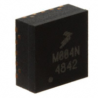
MMG3004NT1
400 - 2200 MHz, 16 dB 27 dBm InGaP HBT
CASE 1543 - 03 PQFN 5x5 PLASTIC
Table 1. Typical Performance (1)
Characteristic Small - Signal Gain (S21) Input Return Loss (S11) Output Return Loss (S22) Power Output @1dB Compression Third Order Output Intercept Point Symbol Gp IRL ORL P1db IP3 900 MHz 19.5 - 7.5 - 10 27 44 1960 MHz 16.5 -8 - 12 27 44 2140 MHz 16 -8 - 12 27 44 Unit dB dB dB dBm dBm
Table 2. Maximum Ratings
Rating Supply Voltage Supply Current RF Input Power Storage Temperature Range Junction Temperature (2) Symbol VDC IDC Pin Tstg TJ Value 6 400 18 - 65 to +150 150 Unit V mA dBm °C °C
2. For reliable operation, the junction temperature should not exceed 150°C.
1. VDC = 5 Vdc, TC = 25°C, 50 ohm system
Table 3. Thermal Characteristics (VDC = 5 Vdc, IDC = 250 mA, TC = 25°C)
Characteristic Thermal Resistance, Junction to Case Symbol RθJC Value (3) 33 Unit °C/W
3. Refer to AN1955, Thermal Measurement Methodology of RF Power Amplifiers. Go to http://www.freescale.com/rf . Select Documentation/Application Notes - AN1955.
© Freescale Semiconductor, Inc., 2005-2008. All rights reserved.
MMG3004NT1 1
RF Device Data Freescale Semiconductor
�Table 4. Electrical Characteristics (VDC = 5 Vdc, 2140 MHz, TC = 25°C, 50 ohm system, in Freescale Application Circuit)
Characteristic Small - Signal Gain (S21) Input Return Loss (S11) Output Return Loss (S22) Power Output @ 1dB Compression Third Order Output Intercept Point Noise Figure Supply Current (1) Supply Voltage (1) Symbol Gp IRL ORL P1dB IP3 NF IDC VDC Min 15 — — — — — 225 — Typ 16 -8 - 12 27 44 3.4 250 5 Max — — — — — — 275 — Unit dB dB dB dBm dBm dB mA V
1. For reliable operation, the junction temperature should not exceed 150°C.
MMG3004NT1 2 RF Device Data Freescale Semiconductor
�Table 5. Functional Pin Description
Name RFin RFout/ VCC VCC VBA GND Pin Number 2, 3, 4 10, 11, 12 14 16 Backside Center Metal Description VBA RF input for the power amplifier. This pin is DC - coupled and requires a DC - blocking series capacitor. RF output for the power amplifier. This pin is DC - coupled and requires a DC - blocking series capacitor. Collector voltage supply. Bias voltage supply. The center metal base of the PQFN package provides both DC and RF ground as well as heat sink contact for the power amplifier. RFin RFin RFin 1 2 3 4 5 6 7 8 16 15 VCC 14 13 12 11 10 9 RFout/VCC RFout/VCC RFout/VCC
(Top View)
Figure 1. Pin Connections
Table 6. ESD Protection Characteristics
Test Methodology Human Body Model (per JESD 22 - A114) Machine Model (per EIA/JESD 22 - A115) Charge Device Model (per JESD 22 - C101) Class 1B (Minimum) A (Minimum) III (Minimum)
Table 7. Moisture Sensitivity Level
Test Methodology Per JESD 22 - A113, IPC/JEDEC J - STD - 020 Rating 3 Package Peak Temperature 260 Unit °C
MMG3004NT1 RF Device Data Freescale Semiconductor 3
�50 OHM TYPICAL CHARACTERISTICS
300 ICC, COLLECTOR CURRENT (mA) 250 200 150 100 50 VCC = 5 Vdc 0 0 1 2 3 4 5 VBA, BIAS VOLTAGE (V) 103 120 125 130 135 140 145 150 TJ, JUNCTION TEMPERATURE (°C) NOTE: The MTTF is calculated with VDC = 5 Vdc, IDC = 250 mA MTTF (YEARS) 105 106
104
Figure 2. Collector Current versus Bias Voltage
Figure 3. MTTF versus Junction Temperature
MMG3004NT1 4 RF Device Data Freescale Semiconductor
�50 OHM APPLICATION CIRCUIT: 900 MHz
VSUPPLY R2 R1
C3
C4 1 16 15 14 13 12 Z6 3 4 5 6 DUT 7 8 Z6 Z7 Z8 Z9 PCB 11 10 9 Z7 L1
C5
C6
RF INPUT
2 Z1 C1 C7 C8 Z2 Z3 Z4 L2 Z5
Current Mirror
Z8 L3
Z9
Z10 C2
Z11
RF OUTPUT
C9
C10
Z1, Z11 Z2, Z10 Z3 Z4 Z5
0.140″ 0.060″ 0.192″ 0.055″ 0.084″
x 0.028″ Microstrip x 0.028″ Microstrip x 0.028″ Microstrip x 0.028″ Microstrip x 0.028″ Microstrip
0.089″ x 0.028″ Microstrip 0.051″ x 0.028″ Microstrip 0.055″ x 0.028″ Microstrip 0.112″ x 0.028″ Microstrip Isola FR408, 0.014″, εr = 3.7
Figure 4. 50 Ohm Test Circuit Schematic
Table 8. 50 Ohm Test Circuit Component Designations and Values
Part C1, C2 C3, C5 C4, C6 C7, C8 C9, C10 L1 L2, L3 R1 R2 Description 15 pF Chip Capacitors 0.01 μF Chip Capacitors 0.1 μF Chip Capacitors 2.2 pF Chip Capacitors 1.8 pF Chip Capacitors 33 nH Chip Inductor 3.9 nH Chip Inductors 22 Ω, 1/10 W Chip Resistor 0 Ω, 1/10 W Chip Resistor Part Number ECUV1H150JCV C0603C103J5RAC C0603C104J5RAC 06035J2R2BS 06035J1R8BS LL1608- FSL33NJ LL1608- FSL3N9S CRCW060322R0FKEA CRCW06030000FKEA Manufacturer Panasonic Kemet Kemet AVX AVX Toko Toko Vishay Vishay
MMG3004NT1 RF Device Data Freescale Semiconductor 5
�50 OHM APPLICATION CIRCUIT: 900 MHz
VBA VSUPPLY
R2
R1 C3 C4 RFin L2 L1
C5 C6
RFout
C1
C7
C8
L3
C9
C10
C2
MMG3004/5 Rev. 3
Figure 5. 50 Ohm Test Circuit Component Layout
MMG3004NT1 6 RF Device Data Freescale Semiconductor
�50 OHM TYPICAL CHARACTERISTICS: 900 MHz
21 Gp, SMALL−SIGNAL GAIN (dB) 0
IRL, INPUT RETURN LOSS (dB)
20 TC = 25°C 19 −40°C
−2
−4
85°C
−6 TC = 85°C −8 VDC = 5 Vdc −40°C 25°C
18 VDC = 5 Vdc 17 840 870 900 f, FREQUENCY (MHz) 930 960
−10 840
870
900 f, FREQUENCY (MHz)
930
960
Figure 6. Small - Signal Gain (S21) versus Frequency
Figure 7. Input Return Loss (S11) versus Frequency
−5 P1dB, 1 dB COMPRESSION POINT (dBm) ORL, OUTPUT RETURN LOSS (dB)
29
−7 TC = −40°C −9 25°C −11 85°C
28
TC = 25°C 85°C −40°C
27
26 VDC = 5 Vdc 25 840 870 900 f, FREQUENCY (MHz) 930 960
−13 VDC = 5 Vdc −15 840 870 900 f, FREQUENCY (MHz) 930 960
Figure 8. Output Return Loss (S22) versus Frequency
IP3, THIRD ORDER OUTPUT INTERCEPT POINT (dBm) 47 10
Figure 9. P1dB versus Frequency
45 NF, NOISE FIGURE (dB) TC = 25°C 43 −40°C 85°C
8
6
TC = 85°C −40°C 25°C
41
4
39 VDC = 5 Vdc 1 MHz Tone Spacing 37 840 870 900 f, FREQUENCY (MHz) 930 960
2 VDC = 5 Vdc 0 840 870 900 f, FREQUENCY (MHz) 930 960
Figure 10. Third Order Output Intercept Point versus Frequency
Figure 11. Noise Figure versus Frequency
MMG3004NT1 RF Device Data Freescale Semiconductor 7
�50 OHM TYPICAL CHARACTERISTICS: 900 MHz
ACPR, ADJACENT CHANNEL POWER RATIO (dBc) −30 VDC = 5 Vdc, f = 900 MHz Single−Carrier IS−95, 9 Channel Forward 750 kHz Measurement Offset 30 kHz Measurement Bandwidth ACPR, ADJACENT CHANNEL POWER RATIO (dBc)
−40
−35
VDC = 5 Vdc, f = 900 MHz Single−Carrier IS−95, 9 Channel Forward 885 kHz Measurement Offset 30 kHz Measurement Bandwidth
−50
−40
−45
−60
TC = 85°C 25°C −40°C
−50
−70
TC = 85°C
25°C −40°C 21 23 25 27 29
−55 19
−80 17
19
21
23
25
27
Pout, OUTPUT POWER (dBm)
Pout, OUTPUT POWER (dBm)
Figure 12. IS - 95 Adjacent Channel Power Ratio versus Output Power
Figure 13. IS - 95 Adjacent Channel Power Ratio versus Output Power
MMG3004NT1 8 RF Device Data Freescale Semiconductor
�50 OHM APPLICATION CIRCUIT: 1900 - 2200 MHz
VSUPPLY R2 R1
C3
C4 1 16 15 14 13 12 Z5 3 11 DUT 6 7 8 Z5 Z6 Z7 PCB Z6 Z7 L1
C5
C6
RF INPUT
2 Z1 C1 C7 C8 4 5 Z1, Z9 Z2, Z8 Z3 Z4 0.140″ 0.060″ 0.259″ 0.080″ x 0.028″ Microstrip x 0.028″ Microstrip x 0.028″ Microstrip x 0.028″ Microstrip Z2 Z3 Z4
Current Mirror
Z8 C2
Z9
RF OUTPUT
10 9
C9
C10
0.049″ x 0.028″ Microstrip 0.036″ x 0.028″ Microstrip 0.254″ x 0.028″ Microstrip Isola FR408, 0.014″, εr = 3.7
Figure 14. 50 Ohm Test Circuit Schematic Table 9. 50 Ohm Test Circuit Component Designations and Values
Part C1, C2 C3, C5 C4, C6 C7, C10 C8 C9 L1 R1 R2 Description 15 pF Chip Capacitors 0.01 μF Chip Capacitors 0.1 μF Chip Capacitors 0.5 pF Chip Capacitors 2.7 pF Chip Capacitor 0.8 pF Chip Capacitor 33 nH Chip Inductor 22 Ω, 1/10 W Chip Resistor 0 Ω, 1/10 W Chip Resistor Part Number ECUV1H150JCV C0603C103J5RAC C0603C104J5RAC 06035J0R5BS 06035J2R7BS 06035J0R8BS LL1608- FSL33NJ CRCW060322R0FKEA CRCW06030000FKEA Manufacturer Panasonic Kemet Kemet AVX AVX AVX Toko Vishay Vishay
MMG3004NT1 RF Device Data Freescale Semiconductor 9
�50 OHM APPLICATION CIRCUIT: 1900 - 2200 MHz
VBA VSUPPLY
R2
R1 C3 C4 RFin L1
C5 C6
RFout
C1
C7
C8
C9
C10
C2
MMG3004/5 Rev. 3
Figure 15. 50 Ohm Test Circuit Component Layout
MMG3004NT1 10 RF Device Data Freescale Semiconductor
�50 OHM TYPICAL CHARACTERISTICS: 1900 - 2200 MHz
18 Gp, SMALL−SIGNAL GAIN (dB) 17 16 15 14 13 VDC = 5 Vdc 12 1900 1960 2020 2080 2140 2200 −10 1900 −5
IRL, INPUT RETURN LOSS (dB)
TC = 25°C 85°C
−6
−40°C
−7
−8
TC = 85°C −40°C VDC = 5 Vdc 1960 25°C
−9
f, FREQUENCY (MHz)
2020 2080 f, FREQUENCY (MHz)
2140
2200
Figure 16. Small - Signal Gain (S21) versus Frequency
Figure 17. Input Return Loss (S11) versus Frequency
−5 P1dB, 1 dB COMPRESSION POINT (dBm) ORL, OUTPUT RETURN LOSS (dB)
29
−7
28 TC = −40°C 27 25°C 26 VDC = 5 Vdc 25 1900 1960 2020 2080 2140 2200 85°C
−9
−11
TC = −40°C
−13 VDC = 5 Vdc −15 1900 1960 2020
85°C
25°C 2080 2140 2200
f, FREQUENCY (MHz)
f, FREQUENCY (MHz)
Figure 18. Output Return Loss (S22) versus Frequency
IP3, THIRD ORDER OUTPUT INTERCEPT POINT (dBm) 47 10
Figure 19. P1dB versus Frequency
45 TC = 25°C 43 −40°C 41 85°C VDC = 5 Vdc 1 MHz Tone Spacing 37 1900 1960 2020 2080 2140 2200 NF, NOISE FIGURE (dB)
8
6 TC = 85°C −40°C VDC = 5 Vdc 0 1900 1960 2020 2080
4
39
2
25°C
2140
2200
f, FREQUENCY (MHz)
f, FREQUENCY (MHz)
Figure 20. Third Order Output Intercept Point versus Frequency
Figure 21. Noise Figure versus Frequency
MMG3004NT1 RF Device Data Freescale Semiconductor 11
�50 OHM TYPICAL CHARACTERISTICS: 1900 - 2200 MHz
ACPR, ADJACENT CHANNEL POWER RATIO (dBc) −30 VDC = 5 Vdc, f = 1960 MHz Single−Carrier IS−95, 9 Channel Forward 750 kHz Measurement Offset 30 kHz Measurement Bandwidth ACPR, ADJACENT CHANNEL POWER RATIO (dBc)
−40
−35
VDC = 5 Vdc, f = 1960 MHz Single−Carrier IS−95, 9 Channel Forward 885 kHz Measurement Offset 30 kHz Measurement Bandwidth
−50
−40
−45 TC = 85°C −50 −55 19 −40°C 25°C 21 23 25 27 29
−60
TC = 85°C 25°C −40°C
−70
−80 17
19
21
23
25
27
Pout, OUTPUT POWER (dBm)
Pout, OUTPUT POWER (dBm)
Figure 22. IS - 95 Adjacent Channel Power Ratio versus Output Power
Figure 23. IS - 95 Adjacent Channel Power Ratio versus Output Power
ACPR, ADJACENT CHANNEL POWER RATIO (dBc)
−20
−30
−40 85°C −50
TC = −40°C
25°C VDC = 5 Vdc, f = 2140 MHz Single−Carrier W−CDMA, 3.84 MHz Channel Bandwidth Input Signal PAR = 8.5 dB @ 0.01% Probability (CCDF) 16 18 20 22 24 26
−60
−70
Pout, OUTPUT POWER (dBm)
Figure 24. Single - Carrier W - CDMA Adjacent Channel Power Ratio versus Output Power
MMG3004NT1 12 RF Device Data Freescale Semiconductor
�50 OHM TYPICAL CHARACTERISTICS
Table 10. Common Emitter S - Parameters (VDC = 5 Vdc, IDC = 250 mA, TC = 25°C, 50 Ohm System)
f MHz 400 425 450 475 500 525 550 575 600 625 650 675 700 725 750 775 800 825 850 875 900 925 950 975 1000 1025 1050 1075 1100 1125 1150 1175 1200 1225 1250 1275 1300 1325 1350 1375 1400 1425 1450 1475 S11 |S11| 0.62780 0.64110 0.65775 0.67009 0.68313 0.69585 0.70558 0.71811 0.72694 0.73704 0.74634 0.75277 0.76214 0.76874 0.77561 0.78327 0.78772 0.79476 0.79893 0.80421 0.80983 0.81256 0.81780 0.82118 0.82354 0.82863 0.82994 0.83369 0.83728 0.83914 0.84333 0.84582 0.84730 0.85017 0.85104 0.85363 0.85515 0.85660 0.85919 0.85982 0.86102 0.86270 0.86382 0.86525 ∠φ - 155.59 - 156.56 - 157.61 - 158.60 - 159.63 - 160.59 - 161.46 - 162.43 - 163.35 - 164.30 - 165.20 - 166.03 - 166.98 - 167.82 - 168.72 - 169.54 - 170.26 - 171.12 - 171.88 - 172.62 - 173.40 - 174.09 - 174.81 - 175.53 - 176.19 - 176.93 - 177.51 - 178.12 - 178.76 - 179.35 - 179.99 179.42 178.80 178.20 177.63 177.01 176.48 175.94 175.39 174.86 174.26 173.77 173.26 172.73 |S21| 7.75028 7.52200 7.40177 7.20037 7.05567 6.91538 6.69940 6.60437 6.42427 6.29327 6.17990 5.99028 5.91391 5.76815 5.64770 5.56291 5.40401 5.33575 5.21557 5.09417 5.04484 4.90083 4.83208 4.75850 4.64462 4.59813 4.47959 4.41800 4.36819 4.25589 4.21812 4.14782 4.07433 4.03089 3.94928 3.91182 3.84948 3.79124 3.75583 3.68725 3.65116 3.60736 3.55564 3.51922 S21 ∠φ 138.19 135.93 133.81 131.68 129.69 127.76 125.72 123.98 122.18 120.47 118.78 117.13 115.54 114.00 112.56 111.09 109.64 108.25 106.88 105.61 104.35 102.95 101.78 100.63 99.41 98.27 97.05 96.02 95.02 93.92 92.91 91.86 90.84 89.88 88.92 87.97 86.97 86.09 85.18 84.24 83.37 82.44 81.56 80.69 |S12| 0.01341 0.01318 0.01297 0.01282 0.01265 0.01255 0.01251 0.01243 0.01240 0.01238 0.01241 0.01246 0.01249 0.01254 0.01262 0.01272 0.01285 0.01299 0.01314 0.01326 0.01340 0.01357 0.01377 0.01398 0.01421 0.01449 0.01482 0.01512 0.01522 0.01522 0.01532 0.01540 0.01549 0.01563 0.01581 0.01603 0.01623 0.01644 0.01665 0.01685 0.01708 0.01733 0.01754 0.01778 S12 ∠φ - 20.61 - 18.49 - 16.33 - 14.50 - 12.50 - 10.52 - 8.66 - 6.84 - 5.19 - 3.35 - 1.68 - 0.10 1.32 2.86 4.27 5.73 7.01 8.22 9.31 10.44 11.44 12.52 13.37 14.40 15.20 15.97 16.45 16.27 16.04 16.13 16.71 17.23 17.85 18.56 19.15 19.78 20.21 20.62 21.10 21.41 21.83 22.12 22.31 22.70 |S22| 0.73308 0.73263 0.73058 0.72961 0.72804 0.72718 0.72650 0.72500 0.72458 0.72338 0.72241 0.72250 0.72135 0.72103 0.72003 0.71950 0.71888 0.71803 0.71838 0.71707 0.71668 0.71611 0.71547 0.71514 0.71375 0.71292 0.71160 0.71100 0.71111 0.71104 0.71144 0.71102 0.71091 0.71058 0.70945 0.70911 0.70802 0.70758 0.70645 0.70534 0.70492 0.70407 0.70310 0.70185 S22 ∠φ 177.59 177.05 176.51 176.03 175.54 175.02 174.46 173.90 173.43 172.92 172.43 171.98 171.44 170.97 170.51 170.03 169.54 169.01 168.59 168.13 167.64 167.14 166.62 166.17 165.68 165.18 164.72 164.34 163.96 163.46 162.96 162.41 161.96 161.46 160.92 160.44 159.92 159.44 158.93 158.44 157.95 157.43 156.95 156.45 (continued)
MMG3004NT1 RF Device Data Freescale Semiconductor 13
�50 OHM TYPICAL CHARACTERISTICS
Table 10. Common Emitter S - Parameters (VDC = 5 Vdc, IDC = 250 mA, TC = 25°C, 50 Ohm System) (continued)
f MHz 1500 1525 1550 1575 1600 1625 1650 1675 1700 1725 1750 1775 1800 1825 1850 1875 1900 1925 1950 1975 2000 2025 2050 2075 2100 2125 2150 2175 2200 2225 2250 2275 2300 2325 2350 2375 2400 2425 2450 2475 2500 2525 2550 2575 S11 |S11| 0.86447 0.86543 0.86646 0.86663 0.86864 0.86848 0.86907 0.86995 0.86908 0.87075 0.87075 0.87095 0.87210 0.87206 0.87291 0.87225 0.87269 0.87341 0.87288 0.87403 0.87359 0.87242 0.87347 0.87337 0.87327 0.87318 0.87233 0.87291 0.87284 0.87305 0.87252 0.87193 0.87178 0.87159 0.87191 0.87202 0.87117 0.87077 0.87026 0.87003 0.86985 0.86940 0.86918 0.86921 ∠φ 171.75 171.19 170.67 170.18 169.65 169.14 168.58 168.06 167.55 166.99 166.48 165.94 165.38 164.86 164.26 163.73 163.18 162.62 162.11 161.54 160.98 160.38 159.78 159.25 158.66 158.11 157.55 156.95 156.41 155.87 155.28 154.76 154.15 153.64 153.13 152.60 152.09 151.53 151.02 150.54 150.02 149.49 148.98 148.48 |S21| 3.49706 3.46774 3.42587 3.38624 3.35249 3.31471 3.28145 3.24680 3.21301 3.17917 3.14872 3.11816 3.08624 3.05732 3.02693 2.99956 2.97218 2.94317 2.91922 2.88985 2.86616 2.84227 2.81763 2.79570 2.77239 2.75232 2.73039 2.70958 2.69236 2.67297 2.65614 2.63741 2.62034 2.60593 2.59024 2.57507 2.55841 2.54515 2.53215 2.51806 2.50328 2.49003 2.47736 2.46415 S21 ∠φ 79.68 78.76 77.92 77.08 76.23 75.38 74.52 73.68 72.89 72.07 71.28 70.46 69.66 68.88 68.07 67.29 66.53 65.76 65.01 64.24 63.49 62.70 61.98 61.26 60.53 59.81 59.07 58.40 57.69 57.01 56.29 55.58 54.89 54.19 53.50 52.78 52.08 51.37 50.65 49.95 49.24 48.49 47.77 47.02 |S12| 0.01815 0.01841 0.01868 0.01889 0.01916 0.01940 0.01966 0.01990 0.02016 0.02043 0.02072 0.02101 0.02127 0.02156 0.02183 0.02214 0.02241 0.02272 0.02300 0.02333 0.02366 0.02397 0.02429 0.02465 0.02498 0.02536 0.02571 0.02602 0.02636 0.02672 0.02709 0.02744 0.02777 0.02812 0.02850 0.02891 0.02926 0.02967 0.03007 0.03047 0.03087 0.03126 0.03167 0.03208 S12 ∠φ 22.78 22.92 23.04 23.19 23.38 23.47 23.55 23.70 23.85 23.94 23.94 24.02 24.02 24.07 24.07 24.03 24.07 24.05 24.10 23.99 23.91 23.80 23.70 23.66 23.49 23.32 23.11 22.93 22.73 22.55 22.23 22.01 21.74 21.52 21.34 21.08 20.77 20.45 20.15 19.77 19.40 18.98 18.61 18.11 |S22| 0.69775 0.69678 0.69558 0.69453 0.69264 0.69185 0.69110 0.68960 0.68912 0.68700 0.68638 0.68533 0.68377 0.68284 0.68136 0.68073 0.67941 0.67817 0.67684 0.67500 0.67393 0.67298 0.67159 0.67018 0.66901 0.66790 0.66702 0.66610 0.66519 0.66417 0.66378 0.66344 0.66387 0.66363 0.66365 0.66346 0.66342 0.66386 0.66405 0.66432 0.66490 0.66538 0.66582 0.66531 S22 ∠φ 156.18 155.64 155.13 154.61 154.06 153.54 153.02 152.47 152.02 151.51 151.05 150.57 150.09 149.66 149.22 148.79 148.37 147.93 147.54 147.15 146.75 146.42 146.04 145.69 145.36 145.01 144.69 144.37 144.03 143.67 143.30 142.95 142.57 142.19 141.75 141.32 140.87 140.39 139.92 139.41 138.85 138.34 137.78 137.21 (continued)
MMG3004NT1 14 RF Device Data Freescale Semiconductor
�50 OHM TYPICAL CHARACTERISTICS
Table 10. Common Emitter S - Parameters (VDC = 5 Vdc, IDC = 250 mA, TC = 25°C, 50 Ohm System) (continued)
f MHz 2600 2625 2650 2675 2700 2725 2750 2775 2800 2825 2850 2875 2900 2925 2950 2975 3000 S11 |S11| 0.86804 0.86808 0.86755 0.86741 0.86769 0.86693 0.86730 0.86724 0.86702 0.86694 0.86602 0.86701 0.86649 0.86653 0.86661 0.86565 0.86627 ∠φ 147.97 147.46 146.99 146.47 145.97 145.47 144.92 144.42 143.87 143.37 142.83 142.28 141.70 141.16 140.59 140.01 139.42 |S21| 2.45098 2.43657 2.42271 2.41111 2.39656 2.38409 2.37136 2.35811 2.34590 2.33197 2.32062 2.30727 2.29559 2.28517 2.27190 2.26115 2.24868 S21 ∠φ 46.28 45.54 44.82 44.06 43.31 42.57 41.82 41.07 40.30 39.55 38.80 38.05 37.30 36.51 35.74 34.97 34.20 |S12| 0.03246 0.03287 0.03328 0.03360 0.03402 0.03438 0.03473 0.03504 0.03530 0.03566 0.03594 0.03623 0.03650 0.03678 0.03700 0.03725 0.03747 S12 ∠φ 17.66 17.21 16.67 16.15 15.56 15.04 14.40 13.77 13.25 12.69 12.05 11.45 10.82 10.22 9.61 9.07 8.51 |S22| 0.66588 0.66553 0.66525 0.66520 0.66461 0.66448 0.66407 0.66312 0.66208 0.66088 0.66087 0.65952 0.65833 0.65713 0.65548 0.65458 0.65272 S22 ∠φ 136.62 136.01 135.46 134.87 134.26 133.68 133.13 132.57 132.00 131.39 130.80 130.25 129.72 129.15 128.55 127.97 127.41
MMG3004NT1 RF Device Data Freescale Semiconductor 15
�2.2 x 2.2
1.35
0.6 2.6 0.8 5.3
NOTES: 1. THERMAL AND RF GROUNDING CONSIDERATIONS SHOULD BE USED IN PCB LAYOUT DESIGN. 2. DEPENDING ON PCB DESIGN RULES, AS MANY VIAS AS POSSIBLE SHOULD BE PLACED ON THE BACKSIDE CENTER METAL GROUND LANDING PATTERN. 3. REFER TO FREESCALE APPLICATION NOTE AN2467 FOR ADDITIONAL PQFN PCB GUIDELINES.
Figure 25. Recommended Mounting Configuration
MMG3004NT1 16 RF Device Data Freescale Semiconductor
�PACKAGE DIMENSIONS
MMG3004NT1 RF Device Data Freescale Semiconductor 17
�MMG3004NT1 18 RF Device Data Freescale Semiconductor
�MMG3004NT1 RF Device Data Freescale Semiconductor 19
�PRODUCT DOCUMENTATION
Refer to the following documents to aid your design process. Application Notes • AN1955: Thermal Measurement Methodology of RF Power Amplifiers • AN3100: General Purpose Amplifier Biasing
REVISION HISTORY
The following table summarizes revisions to this document.
Revision 2 Date Mar. 2007 Description • Replaced Case Outline 1543 - 02 with updated 1543 - 03, Issue C, p. 1, 16 - 18 • Added VCC callout to Pin Connections 10, 11, and 12 in Fig. 1, Pin Connections, p. 3 • Updated Part Numbers in Table 8, Component Designations and Values, 900 MHz, to RoHS compliant part numbers, p. 5 • Corrected circuit board callouts, Vp to VBA and VCC to VSUPPLY, Fig. 5, 50 Ohm Test Circuit Component Layout, 900 MHz, p. 6 • Removed IDC value due to its variability over temperature, Figs. 12 - 13, IS - 95 Adjacent Channel Power Ratio versus Output Power, 900 MHz, p. 8 • Updated Part Numbers in Table 9, Component Designations and Values, 1900 - 2200 MHz, to RoHS compliant part numbers, p. 9 • Corrected circuit board callouts, Vp to VBA and VCC to VSUPPLY, Fig. 15, 50 Ohm Test Circuit Component Layout, 1900 - 2200 MHz, p. 10 • Removed IDC value due to its variability over temperature, Figs. 22 - 23, IS - 95 Adjacent Channel Power Ratio versus Output Power, 1900 - 2200 MHz, and Fig. 24, Single - Carrier W - CDMA Adjacent Channel Power Ratio versus Output Power, 1900 - 2200 MHz, p. 12 • Replaced Table 10, S - Parameters, p. 13 - 15 • Added Product Documentation and Revision History, p. 19 3 Mar. 2008 • Corrected Tape and Reel information from 12 mm, 7 inch Reel to 16 mm, 13 inch Reel, p. 1 • Removed Footnote 2, Continuous voltage and current applied to device, from Table 2, Maximum Ratings, p. 1 • Corrected Fig. 24, Single - Carrier W - CDMA Adjacent Channel Power Ratio versus Output Power y - axis (ACPR) unit of measure to dBc, p. 12
• Corrected S - Parameter table frequency column label to read “MHz” versus “GHz” and corrected frequency values from GHz to MHz, p. 13, 14, 15
MMG3004NT1 20 RF Device Data Freescale Semiconductor
�How to Reach Us:
Home Page: www.freescale.com Web Support: http://www.freescale.com/support USA/Europe or Locations Not Listed: Freescale Semiconductor, Inc. Technical Information Center, EL516 2100 East Elliot Road Tempe, Arizona 85284 +1 - 800 - 521 - 6274 or +1 - 480 - 768 - 2130 www.freescale.com/support Europe, Middle East, and Africa: Freescale Halbleiter Deutschland GmbH Technical Information Center Schatzbogen 7 81829 Muenchen, Germany +44 1296 380 456 (English) +46 8 52200080 (English) +49 89 92103 559 (German) +33 1 69 35 48 48 (French) www.freescale.com/support Japan: Freescale Semiconductor Japan Ltd. Headquarters ARCO Tower 15F 1 - 8 - 1, Shimo - Meguro, Meguro - ku, Tokyo 153 - 0064 Japan 0120 191014 or +81 3 5437 9125 support.japan@freescale.com Asia/Pacific: Freescale Semiconductor Hong Kong Ltd. Technical Information Center 2 Dai King Street Tai Po Industrial Estate Tai Po, N.T., Hong Kong +800 2666 8080 support.asia@freescale.com For Literature Requests Only: Freescale Semiconductor Literature Distribution Center P.O. Box 5405 Denver, Colorado 80217 1 - 800 - 441 - 2447 or 303 - 675 - 2140 Fax: 303 - 675 - 2150 LDCForFreescaleSemiconductor@hibbertgroup.com
Information in this document is provided solely to enable system and software implementers to use Freescale Semiconductor products. There are no express or implied copyright licenses granted hereunder to design or fabricate any integrated circuits or integrated circuits based on the information in this document. Freescale Semiconductor reserves the right to make changes without further notice to any products herein. Freescale Semiconductor makes no warranty, representation or guarantee regarding the suitability of its products for any particular purpose, nor does Freescale Semiconductor assume any liability arising out of the application or use of any product or circuit, and specifically disclaims any and all liability, including without limitation consequential or incidental damages. “Typical” parameters that may be provided in Freescale Semiconductor data sheets and/or specifications can and do vary in different applications and actual performance may vary over time. All operating parameters, including “Typicals”, must be validated for each customer application by customer’s technical experts. Freescale Semiconductor does not convey any license under its patent rights nor the rights of others. Freescale Semiconductor products are not designed, intended, or authorized for use as components in systems intended for surgical implant into the body, or other applications intended to support or sustain life, or for any other application in which the failure of the Freescale Semiconductor product could create a situation where personal injury or death may occur. Should Buyer purchase or use Freescale Semiconductor products for any such unintended or unauthorized application, Buyer shall indemnify and hold Freescale Semiconductor and its officers, employees, subsidiaries, affiliates, and distributors harmless against all claims, costs, damages, and expenses, and reasonable attorney fees arising out of, directly or indirectly, any claim of personal injury or death associated with such unintended or unauthorized use, even if such claim alleges that Freescale Semiconductor was negligent regarding the design or manufacture of the part. Freescalet and the Freescale logo are trademarks of Freescale Semiconductor, Inc. All other product or service names are the property of their respective owners. © Freescale Semiconductor, Inc. 2005-2008. All rights reserved.
MMG3004NT1
Document Number: RF Device Data MMG3004NT1 Rev. 3, 3/2008 Freescale Semiconductor
21
�