Freescale Semiconductor Technical Data
Document Number: MMG3007NT1 Rev. 5, 3/2008
Heterojunction Bipolar Transistor (InGaP HBT)
Broadband High Linearity Amplifier
MMG3007NT1
The MMG3007NT1 is a General Purpose Amplifier that is internally input and output matched. It is designed for a broad range of Class A, small - signal, high linearity, general purpose applications. It is suitable for applications with frequencies from 0 to 6000 MHz such as Cellular, P C S , B W A , W L L , P H S , C AT V, V H F, U H F, U M T S a n d g e n e r a l small - signal RF. Features • Frequency: 0 to 6000 MHz • P1dB: 16 dBm @ 900 MHz • Small - Signal Gain: 19 dB @ 900 MHz • Third Order Output Intercept Point: 30 dBm @ 900 MHz • Single 5 Volt Supply • Internally Matched to 50 Ohms • Low Cost SOT - 89 Surface Mount Package • RoHS Compliant • In Tape and Reel. T1 Suffix = 1000 Units per 12 mm, 7 inch Reel.
0 - 6000 MHz, 19 dB 16 dBm InGaP HBT
12
3
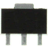
CASE 1514 - 02, STYLE 1 SOT - 89 PLASTIC
Table 1. Typical Performance (1)
Characteristic Small - Signal Gain (S21) Input Return Loss (S11) Output Return Loss (S22) Power Output @1dB Compression Third Order Output Intercept Point Symbol Gp IRL ORL P1db IP3 900 MHz 19 - 14 - 20 16 30 2140 MHz 16.5 - 21 - 17 15.5 29 3500 MHz 14 - 21 - 25 16 28.5 Unit dB dB dB dBm dBm
Table 2. Maximum Ratings
Rating Supply Voltage Supply Current RF Input Power Storage Temperature Range Junction Temperature
(2)
Symbol VCC ICC Pin Tstg TJ
Value 7 250 10 - 65 to +150 150
Unit V mA dBm °C °C
2. For reliable operation, the junction temperature should not exceed 150°C.
1. VCC = 5 Vdc, TC = 25°C, 50 ohm system
Table 3. Thermal Characteristics (VCC = 5 Vdc, ICC = 47 mA, TC = 25°C)
Characteristic Thermal Resistance, Junction to Case Symbol RθJC Value (3) 77 Unit °C/W
3. Refer to AN1955, Thermal Measurement Methodology of RF Power Amplifiers. Go to http://www.freescale.com/rf . Select Documentation/Application Notes - AN1955.
© Freescale Semiconductor, Inc., 2005-2008. All rights reserved.
MMG3007NT1 1
RF Device Data Freescale Semiconductor
�Table 4. Electrical Characteristics (VCC = 5 Vdc, 900 MHz, TC = 25°C, 50 ohm system, in Freescale Application Circuit)
Characteristic Small - Signal Gain (S21) Input Return Loss (S11) Output Return Loss (S22) Power Output @ 1dB Compression Third Order Output Intercept Point Noise Figure Supply Current (1) Supply Voltage (1) Symbol Gp IRL ORL P1dB IP3 NF ICC VCC Min 18 — — — — — 39 — Typ 19 - 14 - 20 16 30 3.8 47 5 Max — — — — — — 55 — Unit dB dB dB dBm dBm dB mA V
1. For reliable operation, the junction temperature should not exceed 150°C.
MMG3007NT1 2 RF Device Data Freescale Semiconductor
�Table 5. Functional Pin Description
Pin Number 1 2 3 RFin Ground RFout/DC Supply 1 2 3 Pin Function 2
Figure 1. Functional Diagram
Table 6. ESD Protection Characteristics
Test Methodology Human Body Model (per JESD 22 - A114) Machine Model (per EIA/JESD 22 - A115) Charge Device Model (per JESD 22 - C101) Class 1A (Minimum) A (Minimum) IV (Minimum)
Table 7. Moisture Sensitivity Level
Test Methodology Per JESD 22 - A113, IPC/JEDEC J - STD - 020 Rating 1 Package Peak Temperature 260 Unit °C
MMG3007NT1 RF Device Data Freescale Semiconductor 3
�50 OHM TYPICAL CHARACTERISTICS
25 Gp, SMALL−SIGNAL GAIN (dB) 0
TC = 85°C 20 - 40°C 15
25°C S11, S22 (dB)
−10 S22 −20
S11 −30 VCC = 5 Vdc VCC = 5 Vdc ICC = 47 mA −40 0 1 2 f, FREQUENCY (GHz) 3 4 0 1 2 f, FREQUENCY (GHz) 3 4
10
Figure 2. Small - Signal Gain (S21) versus Frequency
Figure 3. Input/Output Return Loss versus Frequency
23 P1dB, 1 dB COMPRESSION POINT (dBm) 21 900 MHz 19 1960 MHz 17 15 13 11 9 8 9 10 11 12 13 14 15 16 Pout, OUTPUT POWER (dBm) 2600 MHz 3500 MHz VCC = 5 Vdc ICC = 47 mA 2140 MHz
20 19 18 17 16 15 14 13 0.5 1 1.5 2 2.5 3 3.5 f, FREQUENCY (GHz) VCC = 5 Vdc ICC = 47 mA
Gp, SMALL−SIGNAL GAIN (dB)
Figure 4. Small - Signal Gain versus Output Power
IP3, THIRD ORDER OUTPUT INTERCEPT POINT (dBm) 100 ICC, COLLECTOR CURRENT (mA) 33
Figure 5. P1dB versus Frequency
80
30
60
27
40
24 VCC = 5 Vdc ICC = 47 mA 1 MHz Tone Spacing 0 1 2 f, FREQUENCY (GHz) 3 4
20
21
0 4 4.2 4.4 4.6 4.8 5 5.2 5.4 VCC, COLLECTOR VOLTAGE (V)
18
Figure 6. Collector Current versus Collector Voltage
Figure 7. Third Order Output Intercept Point versus Frequency
MMG3007NT1 4 RF Device Data Freescale Semiconductor
�50 OHM TYPICAL CHARACTERISTICS
IP3, THIRD ORDER OUTPUT INTERCEPT POINT (dBm) 36 IP3, THIRD ORDER OUTPUT INTERCEPT POINT (dBm) 32 31 30 29 28 27 26 25 −40 VCC = 5 Vdc f = 900 MHz 1 MHz Tone Spacing −20 0 20 40 60 80 100
33
30
27
24 f = 900 MHz 1 MHz Tone Spacing 21 4.9 4.95 5 5.05 5.1 VCC, COLLECTOR VOLTAGE (V)
T, TEMPERATURE (_C)
Figure 8. Third Order Output Intercept Point versus Collector Voltage
Figure 9. Third Order Output Intercept Point versus Case Temperature
−30 IMD, THIRD ORDER INTERMODULATION DISTORTION (dBc) −40 MTTF (YEARS) VCC = 5 Vdc ICC = 47 mA f = 900 MHz 1 MHz Tone Spacing 1 5 9 13
106
105
−50
−60
104
−70
−80 −3
103 120 125 130 135 140 145 150 Pout, OUTPUT POWER (dBm) TJ, JUNCTION TEMPERATURE (°C) NOTE: The MTTF is calculated with VCC = 5 Vdc, ICC = 47 mA
Figure 10. Third Order Intermodulation versus Output Power
ACPR, ADJACENT CHANNEL POWER RATIO (dBc)
Figure 11. MTTF versus Junction Temperature
8
−20 VCC = 5 Vdc ICC = 47 mA f = 2140 MHz Single−Carrier W−CDMA, 3.84 MHz Channel Bandwidth Input Signal PAR = 8.5 dB @ 0.01% Probability (CCDF)
NF, NOISE FIGURE (dB)
6
−30
−40
4
−50
2 VCC = 5 Vdc ICC = 47 mA 0 0 1 2 f, FREQUENCY (GHz) 3 4
−60
−70 −2 0 2 4 6 8 10 12 Pout, OUTPUT POWER (dBm)
Figure 12. Noise Figure versus Frequency
Figure 13. Single - Carrier W - CDMA Adjacent Channel Power Ratio versus Output Power MMG3007NT1
RF Device Data Freescale Semiconductor
5
�50 OHM APPLICATION CIRCUIT: 40- 300 MHz
VSUPPLY
R1
C3 L1 RF INPUT DUT
C4
Z1 C1
Z2
Z3
Z4 C2 Z4 PCB
Z5
RF OUTPUT
VCC
Z1, Z5 Z2 Z3
0.347″ x 0.058″ Microstrip 0.575″ x 0.058″ Microstrip 0.172″ x 0.058″ Microstrip
0.403″ x 0.058″ Microstrip Getek Grade ML200C, 0.031″, εr = 4.1
Figure 14. 50 Ohm Test Circuit Schematic
30 S21 20 S21, S11, S22 (dB) 10 0 −10 −20 −30 S11 −40 0 100 200 300 f, FREQUENCY (MHz) S22 VCC = 5 Vdc ICC = 47 mA 400 500 C1 C4 C3 L1 C2 R1
MMG30XX Rev 2
Figure 15. S21, S11 and S22 versus Frequency
Figure 16. 50 Ohm Test Circuit Component Layout
Table 8. 50 Ohm Test Circuit Component Designations and Values
Part C1, C2, C3 C4 L1 R1 Description 0.01 μF Chip Capacitors 1000 pF Chip Capacitor 470 nH Chip Inductor 0 W Chip Resistor Part Number C0603C103J5RAC C0603C102J5RAC BK2125HM471 - T ERJ3GEY0R00V Manufacturer Kemet Kemet Taiyo Yuden Panasonic
MMG3007NT1 6 RF Device Data Freescale Semiconductor
�50 OHM APPLICATION CIRCUIT: 300 - 3600 MHz
VSUPPLY
R1
C3 L1 RF INPUT DUT
C4
Z1 C1
Z2
Z3
Z4 C2 Z4 PCB
Z5
RF OUTPUT
VCC
Z1, Z5 Z2 Z3
0.347″ x 0.058″ Microstrip 0.575″ x 0.058″ Microstrip 0.172″ x 0.058″ Microstrip
0.403″ x 0.058″ Microstrip Getek Grade ML200C, 0.031″, εr = 4.1
Figure 17. 50 Ohm Test Circuit Schematic
30 20 S21, S11, S22 (dB) 10 0 −10 −20 −30 300 S11 800 1300 1800 2300 2800 3300 3800 MMG30XX Rev 2 VCC = 5 Vdc ICC = 47 mA S22 L1 C1 C2 S21
R1 C4 C3
f, FREQUENCY (MHz)
Figure 18. S21, S11 and S22 versus Frequency
Figure 19. 50 Ohm Test Circuit Component Layout
Table 9. 50 Ohm Test Circuit Component Designations and Values
Part C1, C2 C3 C4 L1 R1 Description 150 pF Chip Capacitors 0.01 μF Chip Capacitor 1000 pF Chip Capacitor 56 nH Chip Inductor 0 W Chip Resistor Part Number C0603C151J5RAC C0603C103J5RAC C0603C102J5RAC HK160856NJ - T ERJ3GEY0R00V Manufacturer Kemet Kemet Kemet Taiyo Yuden Panasonic
MMG3007NT1 RF Device Data Freescale Semiconductor 7
�50 OHM TYPICAL CHARACTERISTICS
Table 10. Common Emitter S - Parameters (VCC = 5 Vdc, ICC = 47 mA, TC = 25°C, 50 Ohm System)
f MHz 100 150 200 250 300 350 400 450 500 550 600 650 700 750 800 850 900 950 1000 1050 1100 1150 1200 1250 1300 1350 1400 1450 1500 1550 1600 1650 1700 1750 1800 1850 1900 1950 2000 2050 2100 2150 2200 2250 S11 |S11| 0.03698 0.0413 0.04475 0.046352 0.048403 0.05 0.0499 0.04922 0.04838 0.04902 0.04911 0.0497 0.05086 0.05247 0.05441 0.05624 0.05818 0.06054 0.06284 0.06676 0.06962 0.07142 0.07473 0.07822 0.08137 0.08501 0.085621 0.08691 0.087447 0.088958 0.088598 0.089575 0.09071 0.0938 0.097 0.10094 0.10562 0.10927 0.11424 0.11811 0.12221 0.12585 0.13197 0.13625 ∠φ 162.744 161.759 159.333 159.222 155.469 151.008 147.696 144.11 141.343 137.521 134.226 130.851 127.93 124.848 122.43 120.786 118.791 117.037 115.852 114.603 113.845 114.019 113.644 113.329 113.158 112.83 112.341 112.503 112.516 110.702 108.771 107.354 105.666 104.101 102.621 101.285 99.475 97.823 96.4 94.531 93.106 91.879 90.391 88.624 |S21| 9.488476 9.431009 9.37615 9.34083 9.29558 9.26495 9.21219 9.16094 9.10787 9.04991 8.98419 8.91939 8.85099 8.78068 8.70765 8.63598 8.5575 8.47718 8.40286 8.31905 8.23305 8.14799 8.05859 7.97269 7.89042 7.80455 7.71693 7.62844 7.55444 7.46781 7.39276 7.30109 7.2314 7.15066 7.07137 6.98725 6.90714 6.83262 6.75439 6.67977 6.60249 6.53055 6.44752 6.37451 S21 ∠φ 175.169 172.714 169.547 167.191 164.704 162.138 159.65 157.234 154.702 152.326 149.922 147.525 145.201 142.838 140.522 138.198 135.918 133.677 131.466 129.243 127.045 124.84 122.666 120.536 118.443 116.374 114.349 112.301 110.29 108.325 106.371 104.406 102.488 100.592 98.688 96.791 94.976 93.117 91.288 89.43 87.648 85.88 84.16 82.389 |S12| 0.07218 0.073936 0.07479 0.0744 0.07458 0.07444 0.07473 0.07499 0.07517 0.07536 0.07567 0.07584 0.07618 0.07642 0.07659 0.07702 0.0774 0.07767 0.07806 0.07848 0.07874 0.07912 0.07962 0.07992 0.08035 0.08077 0.08135 0.08168 0.08226 0.08275 0.08326 0.08366 0.0841 0.08459 0.0851 0.08555 0.08607 0.0865 0.08691 0.08733 0.08781 0.0884 0.08868 0.08924 S12 ∠φ - 0.406 - 0.163 - 1.111 - 1.219 - 1.237 - 1.639 - 1.957 - 2.087 - 2.464 - 2.681 - 2.89 - 3.227 - 3.577 - 3.81 - 4.138 - 4.463 - 4.812 - 5.244 - 5.558 - 5.948 - 6.3 - 6.731 - 7.194 - 7.652 - 8.105 - 8.476 - 8.943 - 9.492 - 9.966 - 10.605 - 11.086 - 11.654 - 12.158 - 12.724 - 13.319 - 13.926 - 14.507 - 15.154 - 15.771 - 16.325 - 17.024 - 17.685 - 18.268 - 18.993 |S22| 0.06601 0.07813 0.089562 0.09748 0.10124 0.10466 0.10811 0.11164 0.11391 0.11765 0.11998 0.12163 0.12411 0.12586 0.12711 0.12825 0.12922 0.13 0.13077 0.13124 0.13158 0.13134 0.13136 0.13147 0.1318 0.13257 0.13274 0.130129 0.127178 0.125783 0.12282 0.1228 0.12308 0.12424 0.12564 0.12718 0.12895 0.13127 0.13415 0.13706 0.14095 0.14488 0.14844 0.15223 S22 ∠φ - 6.062 - 11.706 - 18.834 - 25.724 - 32.775 - 36.946 - 41.977 - 46.631 - 50.846 - 55.096 - 59.312 - 63.354 - 67.411 - 71.332 - 75.244 - 79.297 - 83.181 - 87.373 - 91.474 - 95.143 - 99.674 - 104.011 - 108.404 - 112.847 - 117.291 - 121.809 - 126.4 - 130.945 - 132.429 - 135.873 - 139.82 - 142.9 - 146.866 - 150.805 - 154.586 - 158.448 - 162.5 - 166.07 - 169.355 - 172.886 - 175.782 - 179.155 178.18 175.153 (continued)
MMG3007NT1 8 RF Device Data Freescale Semiconductor
�50 OHM TYPICAL CHARACTERISTICS
Table 10. Common Emitter S - Parameters (VCC = 5 Vdc, ICC = 47 mA, TC = 25°C, 50 Ohm System) (continued)
f MHz 2300 2350 2400 2450 2500 2550 2600 2650 2700 2750 2800 2850 2900 2950 3000 3050 3100 3150 3200 3250 3300 3350 3400 3450 3500 3550 3600 S11 |S11| 0.14158 0.14606 0.15065 0.15511 0.15948 0.16385 0.16854 0.17283 0.17698 0.18126 0.1858 0.18957 0.19403 0.19798 0.20132 0.20676 0.21059 0.21388 0.21774 0.22229 0.22492 0.2287 0.23228 0.2365 0.24039 0.24401 0.24834 ∠φ 86.951 85.398 83.971 82.457 80.991 79.722 78.35 76.864 75.562 74.328 72.976 71.773 70.699 69.575 68.53 67.445 66.347 65.517 64.628 63.76 62.653 61.882 60.924 60.161 59.326 58.457 57.659 |S21| 6.30389 6.23166 6.16179 6.09153 6.02115 5.95767 5.89249 5.82721 5.76221 5.70193 5.64062 5.58104 5.52616 5.46422 5.41159 5.36032 5.30349 5.25234 5.20188 5.15023 5.10104 5.05108 5.00022 4.95117 4.90461 4.85739 4.80824 S21 ∠φ 80.681 78.989 77.288 75.581 73.906 72.273 70.612 68.994 67.358 65.748 64.155 62.533 60.973 59.362 57.778 56.228 54.654 53.104 51.53 49.962 48.396 46.866 45.297 43.756 42.216 40.692 39.155 |S12| 0.08971 0.09007 0.09053 0.09088 0.09142 0.09177 0.09216 0.09255 0.09293 0.09333 0.09391 0.09428 0.09472 0.09518 0.09558 0.09592 0.09653 0.09687 0.09729 0.09771 0.09812 0.09855 0.099 0.09926 0.09948 0.09979 0.10008 S12 ∠φ - 19.632 - 20.321 - 20.98 - 21.711 - 22.394 - 23.024 - 23.702 - 24.506 - 25.194 - 25.926 - 26.671 - 27.402 - 28.203 - 28.947 - 29.733 - 30.462 - 31.263 - 32.035 - 32.944 - 33.702 - 34.531 - 35.414 - 36.284 - 37.17 - 38.046 - 38.943 - 39.768 |S22| 0.15572 0.15962 0.16279 0.16641 0.16996 0.17342 0.17676 0.17953 0.18268 0.18543 0.18837 0.19087 0.19395 0.19629 0.19941 0.20221 0.20477 0.20796 0.21083 0.21442 0.21656 0.22001 0.2241 0.22826 0.23275 0.23669 0.24177 S22 ∠φ 172.537 170.114 167.517 165.072 162.826 160.459 157.989 155.564 153.165 150.629 148.259 145.593 143.044 140.485 137.461 135.101 132.383 129.58 126.913 124.314 121.289 118.535 115.888 113.148 110.547 107.983 105.495
MMG3007NT1 RF Device Data Freescale Semiconductor 9
�1.7 7.62 0.305 diameter
3.48 5.33 1.27 1.27 0.86 0.64 3.86 0.58
2.49
2.54
Recommended Solder Stencil
NOTES: 1. THERMAL AND RF GROUNDING CONSIDERATIONS SHOULD BE USED IN PCB LAYOUT DESIGN. 2. DEPENDING ON PCB DESIGN RULES, AS MANY VIAS AS POSSIBLE SHOULD BE PLACED ON THE LANDING PATTERN. 3. IF VIAS CANNOT BE PLACED ON THE LANDING PATTERN, THEN AS MANY VIAS AS POSSIBLE SHOULD BE PLACED AS CLOSE TO THE LANDING PATTERN AS POSSIBLE FOR OPTIMAL THERMAL AND RF PERFORMANCE. 4. RECOMMENDED VIA PATTERN SHOWN HAS 0.381 x 0.762 MM PITCH.
Figure 20. Recommended Mounting Configuration
MMG3007NT1 10 RF Device Data Freescale Semiconductor
�PACKAGE DIMENSIONS
MMG3007NT1 RF Device Data Freescale Semiconductor 11
�MMG3007NT1 12 RF Device Data Freescale Semiconductor
�MMG3007NT1 RF Device Data Freescale Semiconductor 13
�PRODUCT DOCUMENTATION
Refer to the following documents to aid your design process. Application Notes • AN1955: Thermal Measurement Methodology of RF Power Amplifiers • AN3100: General Purpose Amplifier Biasing
REVISION HISTORY
The following table summarizes revisions to this document.
Revision 3 4 5 Date Mar. 2007 July 2007 Mar. 2008 • • Description Corrected and updated Part Numbers in Tables 8 and 9, Component Designations and Values, to RoHS compliant part numbers, p. 6, 7 Replaced Case Outline 1514 - 01 with 1514 - 02, Issue D, p. 1, 11 - 13. Case updated to add missing dimension for Pin 1 and Pin 3.
• Removed Footnote 2, Continuous voltage and current applied to device, from Table 2, Maximum Ratings, p. 1 • Corrected Fig. 13, Single - Carrier W - CDMA Adjacent Channel Power Ratio versus Output Power y - axis (ACPR) unit of measure to dBc, p. 5
• Corrected S - Parameter table frequency column label to read “MHz” versus “GHz” and corrected frequency values from GHz to MHz, p. 8, 9
MMG3007NT1 14 RF Device Data Freescale Semiconductor
�How to Reach Us:
Home Page: www.freescale.com Web Support: http://www.freescale.com/support USA/Europe or Locations Not Listed: Freescale Semiconductor, Inc. Technical Information Center, EL516 2100 East Elliot Road Tempe, Arizona 85284 +1 - 800 - 521 - 6274 or +1 - 480 - 768 - 2130 www.freescale.com/support Europe, Middle East, and Africa: Freescale Halbleiter Deutschland GmbH Technical Information Center Schatzbogen 7 81829 Muenchen, Germany +44 1296 380 456 (English) +46 8 52200080 (English) +49 89 92103 559 (German) +33 1 69 35 48 48 (French) www.freescale.com/support Japan: Freescale Semiconductor Japan Ltd. Headquarters ARCO Tower 15F 1 - 8 - 1, Shimo - Meguro, Meguro - ku, Tokyo 153 - 0064 Japan 0120 191014 or +81 3 5437 9125 support.japan@freescale.com Asia/Pacific: Freescale Semiconductor Hong Kong Ltd. Technical Information Center 2 Dai King Street Tai Po Industrial Estate Tai Po, N.T., Hong Kong +800 2666 8080 support.asia@freescale.com For Literature Requests Only: Freescale Semiconductor Literature Distribution Center P.O. Box 5405 Denver, Colorado 80217 1 - 800 - 441 - 2447 or 303 - 675 - 2140 Fax: 303 - 675 - 2150 LDCForFreescaleSemiconductor@hibbertgroup.com
Information in this document is provided solely to enable system and software implementers to use Freescale Semiconductor products. There are no express or implied copyright licenses granted hereunder to design or fabricate any integrated circuits or integrated circuits based on the information in this document. Freescale Semiconductor reserves the right to make changes without further notice to any products herein. Freescale Semiconductor makes no warranty, representation or guarantee regarding the suitability of its products for any particular purpose, nor does Freescale Semiconductor assume any liability arising out of the application or use of any product or circuit, and specifically disclaims any and all liability, including without limitation consequential or incidental damages. “Typical” parameters that may be provided in Freescale Semiconductor data sheets and/or specifications can and do vary in different applications and actual performance may vary over time. All operating parameters, including “Typicals”, must be validated for each customer application by customer’s technical experts. Freescale Semiconductor does not convey any license under its patent rights nor the rights of others. Freescale Semiconductor products are not designed, intended, or authorized for use as components in systems intended for surgical implant into the body, or other applications intended to support or sustain life, or for any other application in which the failure of the Freescale Semiconductor product could create a situation where personal injury or death may occur. Should Buyer purchase or use Freescale Semiconductor products for any such unintended or unauthorized application, Buyer shall indemnify and hold Freescale Semiconductor and its officers, employees, subsidiaries, affiliates, and distributors harmless against all claims, costs, damages, and expenses, and reasonable attorney fees arising out of, directly or indirectly, any claim of personal injury or death associated with such unintended or unauthorized use, even if such claim alleges that Freescale Semiconductor was negligent regarding the design or manufacture of the part. Freescalet and the Freescale logo are trademarks of Freescale Semiconductor, Inc. All other product or service names are the property of their respective owners. © Freescale Semiconductor, Inc. 2005-2008. All rights reserved.
MMG3007NT1
Document Number: RF Device Data MMG3007NT1 Rev. 5, 3/2008 Freescale Semiconductor
15
�