Freescale Semiconductor Technical Data
Document Number: MMG3009NT1 Rev. 2, 5/2006
Heterojunction Bipolar Transistor (InGaP HBT)
Broadband High Linearity Amplifier
The MMG3009NT1 is a General Purpose Amplifier that is internally input and output matched. It is designed for a broad range of Class A, small - signal, high linearity, general purpose applications. It is suitable for applications with frequencies from 0 to 6000 MHz such as Cellular, P C S , B W A , W L L , P H S , C AT V, V H F, U H F, U M T S a n d g e n e r a l small - signal RF. Features • Frequency: 0 to 6000 MHz • P1dB: 18 dBm @ 900 MHz • Small - Signal Gain: 15 dB @ 900 MHz • Third Order Output Intercept Point: 34 dBm @ 900 MHz • Single 5 Volt Supply • Internally Matched to 50 Ohms • Low Cost SOT - 89 Surface Mount Package • RoHS Compliant • In Tape and Reel. T1 Suffix = 1000 Units per 12 mm, 7 inch Reel.
MMG3009NT1
0 - 6000 MHz, 15 dB 18 dBm InGaP HBT
12
3
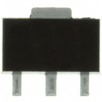
CASE 1514 - 01, STYLE 1 SOT - 89 PLASTIC
Table 1. Typical Performance (1)
Characteristic Small - Signal Gain (S21) Input Return Loss (S11) Output Return Loss (S22) Power Output @1dB Compression Third Order Output Intercept Point Symbol Gp IRL ORL P1db IP3 900 MHz 15 - 13 - 17 18 34 2140 MHz 14 - 26 - 15 18 32 3500 MHz 12.5 - 22 - 24 17.5 31 Unit dB dB dB dBm dBm
Table 2. Maximum Ratings
Rating Supply Voltage Supply Current RF Input Power Storage Temperature Range Junction Temperature
(3) (2) (2)
Symbol VCC ICC Pin Tstg TJ
Value 7 300 10 - 65 to +150 150
Unit V mA dBm °C °C
2. Continuous voltage and current applied to device. 3. For reliable operation, the junction temperature should not exceed 150°C.
1. VCC = 5 Vdc, TC = 25°C, 50 ohm system
Table 3. Thermal Characteristics (VCC = 5 Vdc, ICC = 70 mA, TC = 25°C)
Characteristic Thermal Resistance, Junction to Case Symbol RθJC Value (4) 81 Unit °C/W
4. Refer to AN1955, Thermal Measurement Methodology of RF Power Amplifiers. Go to http://www.freescale.com/rf . Select Documentation/Application Notes - AN1955.
© Freescale Semiconductor, Inc., 2006. All rights reserved.
MMG3009NT1 6-1
Freescale Semiconductor RF Product Device Data
�Table 4. Electrical Characteristics (VCC = 5 Vdc, 900 MHz, TC = 25°C, 50 ohm system, in Freescale Application Circuit)
Characteristic Small - Signal Gain (S21) Input Return Loss (S11) Output Return Loss (S22) Power Output @ 1dB Compression Third Order Output Intercept Point Noise Figure Supply Current (1) Supply Voltage (1) Symbol Gp IRL ORL P1dB IP3 NF ICC VCC Min 14.3 — — — — — 58 — Typ 15 - 13 - 17 18 34 4.2 70 5 Max — — — — — — 82 — Unit dB dB dB dBm dBm dB mA V
1. For reliable operation, the junction temperature should not exceed 150°C.
MMG3009NT1 6-2 Freescale Semiconductor RF Product Device Data
�Table 5. Functional Pin Description
Pin Number 1 2 3 RFin Ground RFout/DC Supply 1 2 3 Pin Function 2
Figure 1. Functional Diagram
Table 6. ESD Protection Characteristics
Test Methodology Human Body Model (per JESD 22 - A114) Machine Model (per EIA/JESD 22 - A115) Charge Device Model (per JESD 22 - C101) Class 1A (Minimum) A (Minimum) IV (Minimum)
Table 7. Moisture Sensitivity Level
Test Methodology Per JESD 22 - A113, IPC/JEDEC J - STD - 020 Rating 1 Package Peak Temperature 260 Unit °C
MMG3009NT1 Freescale Semiconductor RF Product Device Data 6-3
�50 OHM TYPICAL CHARACTERISTICS
20 Gp, SMALL−SIGNAL GAIN (dB) TC = 85°C 15 −40°C 25°C S11, S22 (dB) 0
−10 S11
−20 S22 −30
10
VCC = 5 Vdc 5 0 1 2 f, FREQUENCY (GHz) 3 4 −40 0 1 2 f, FREQUENCY (GHz) 3
VCC = 5 Vdc ICC = 70 mA 4
Figure 2. Small - Signal Gain (S21) versus Frequency
Figure 3. Input/Output Return Loss versus Frequency
21 P1dB, 1 dB COMPRESSION POINT (dBm) 19 17 900 MHz 15 13 11 9 7 10 12 14 16 Pout, OUTPUT POWER (dBm) 3500 MHz 2600 MHz VCC = 5 Vdc ICC = 70 mA 18 20 1960 MHz 2140 MHz
20 19 18 17 16 15 14 13 0.5 1 1.5 2 2.5 3 3.5 f, FREQUENCY (GHz) VCC = 5 Vdc ICC = 70 mA
Gp, SMALL−SIGNAL GAIN (dB)
Figure 4. Small - Signal Gain versus Output Power
IP3, THIRD ORDER OUTPUT INTERCEPT POINT (dBm) 100 ICC, COLLECTOR CURRENT (mA) 36
Figure 5. P1dB versus Frequency
80
33
60
30
40
27 VCC = 5 Vdc ICC = 70 mA 1 MHz Tone Spacing 0 1 2 f, FREQUENCY (GHz) 3 4
20
24
0 4 4.2 4.4 4.6 4.8 5 5.2 5.4 VCC, COLLECTOR VOLTAGE (V)
21
Figure 6. Collector Current versus Collector Voltage
Figure 7. Third Order Output Intercept Point versus Frequency
MMG3009NT1 6-4 Freescale Semiconductor RF Product Device Data
�50 OHM TYPICAL CHARACTERISTICS
IP3, THIRD ORDER OUTPUT INTERCEPT POINT (dBm) 36 IP3, THIRD ORDER OUTPUT INTERCEPT POINT (dBm) 35 34 33 32 31 30 29 28 −40 VCC = 5 Vdc f = 900 MHz 1 MHz Tone Spacing −20 0 20 40 60 80 100
33
30
27
24 f = 900 MHz 1 MHz Tone Spacing 21 4.9 4.95 5 5.05 5.1 VCC, COLLECTOR VOLTAGE (V)
T, TEMPERATURE (_C)
Figure 8. Third Order Output Intercept Point versus Collector Voltage
Figure 9. Third Order Output Intercept Point versus Case Temperature
−30 IMD, THIRD ORDER INTERMODULATION DISTORTION (dBc) −40 MTTF (YEARS) VCC = 5 Vdc ICC = 70 mA f = 900 MHz 1 MHz Tone Spacing
105
−50
104
−60
−70
−80 0 3 6 9 12 15 Pout, OUTPUT POWER (dBm)
103 120 125 130 135 140 145 150 TJ, JUNCTION TEMPERATURE (°C) NOTE: The MTTF is calculated with VCC = 5 Vdc, ICC = 70 mA
Figure 10. Third Order Intermodulation versus Output Power
Figure 11. MTTF versus Junction Temperature
ACPR, ADJACENT CHANNEL POWER RATIO (dB)
8
−20 VCC = 5 Vdc ICC = 70 mA f = 2140 MHz Single−Carrier W−CDMA, 3.84 MHz Channel Bandwidth PAR = 8.5 dB @ 0.01% Probability (CCDF)
NF, NOISE FIGURE (dB)
6
−30
−40
4
−50
2 VCC = 5 Vdc ICC = 70 mA 0 0 1 2 f, FREQUENCY (GHz) 3 4
−60
−70 2 4 6 8 10 12 14 16 Pout, OUTPUT POWER (dBm)
Figure 12. Noise Figure versus Frequency
Figure 13. Single - Carrier W - CDMA Adjacent Channel Power Ratio versus Output Power MMG3009NT1
Freescale Semiconductor RF Product Device Data
6-5
�50 OHM APPLICATION CIRCUIT: 40- 300 MHz
VSUPPLY
R1
C3 L1 RF INPUT DUT
C4
Z1 C1
Z2
Z3
Z4 C2 Z4 PCB
Z5
RF OUTPUT
VCC
Z1, Z5 Z2 Z3
0.347″ x 0.058″ Microstrip 0.575″ x 0.058″ Microstrip 0.172″ x 0.058″ Microstrip
0.403″ x 0.058″ Microstrip Getek Grade ML200C, 0.031″, εr = 4.1
Figure 14. 50 Ohm Test Circuit Schematic
20 10 S21, S11, S22 (dB) 0 −10 S22 −20 −30 −40 0 C1 L1 C2 S21
R1 C4 C3
VCC = 5 Vdc ICC = 70 mA 100 200
S11 300 400 500
MMG30XX Rev 2
f, FREQUENCY (MHz)
Figure 15. S21, S11 and S22 versus Frequency
Figure 16. 50 Ohm Test Circuit Component Layout
Table 8. 50 Ohm Test Circuit Component Designations and Values
Part C1, C2, C3 C4 L1 R1 Description 0.01 μF Chip Capacitors 1000 pF Chip Capacitor 470 nH Chip Inductor 0 W Chip Resistor Part Number 0603A103JAT2A 0603A102JAT2A BK2125HM471 ERJ3GEY0R00V Manufacturer AVX AVX Taiyo Yuden Panasonic
MMG3009NT1 6-6 Freescale Semiconductor RF Product Device Data
�50 OHM APPLICATION CIRCUIT: 300 - 3600 MHz
VSUPPLY
R1
C3 L1 RF INPUT DUT
C4
Z1 C1
Z2
Z3
Z4 C2 Z4 PCB
Z5
RF OUTPUT
VCC
Z1, Z5 Z2 Z3
0.347″ x 0.058″ Microstrip 0.575″ x 0.058″ Microstrip 0.172″ x 0.058″ Microstrip
0.403″ x 0.058″ Microstrip Getek Grade ML200C, 0.031″, εr = 4.1
Figure 17. 50 Ohm Test Circuit Schematic
30 20 S21, S11, S22 (dB) 10 0 C1 −10 −20 S22 VCC = 5 Vdc ICC = 70 mA 800 1300 L1 C2
S21
R1 C4 C3
S11 1800 2300 2800 3300 3800
−30 300
MMG30XX Rev 2
f, FREQUENCY (MHz)
Figure 18. S21, S11 and S22 versus Frequency
Figure 19. 50 Ohm Test Circuit Component Layout
Table 9. 50 Ohm Test Circuit Component Designations and Values
Part C1, C2 C3 C4 L1 R1 Description 150 pF Chip Capacitors 0.01 μF Chip Capacitor 1000 pF Chip Capacitor 56 nH Chip Inductor 0 W Chip Resistor Part Number 06035A151JAT2A 0603A103JAT2A 0603A102JAT2A HK160856NJ - T ERJ3GEY0R00V Manufacturer AVX AVX AVX Taiyo Yuden Panasonic
MMG3009NT1 Freescale Semiconductor RF Product Device Data 6-7
�50 OHM TYPICAL CHARACTERISTICS
Table 10. Class A Common Emitter S - Parameters at VCC = 5 Vdc, ICC = 70 mA, TC = 255C
f GHz 0.1 0.15 0.2 0.25 0.3 0.35 0.4 0.45 0.5 0.55 0.6 0.65 0.7 0.75 0.8 0.85 0.9 0.95 1.0 1.05 1.1 1.15 1.2 1.25 1.3 1.35 1.4 1.45 1.5 1.55 1.6 1.65 1.7 1.75 1.8 1.85 1.9 1.95 2.0 2.05 2.1 2.15 2.2 2.25 2.3 2.35 S11 |S11| 0.19606 0.19734 0.19944 0.20027 0.19924 0.19543 0.19419 0.19172 0.18914 0.18788 0.18596 0.18399 0.18285 0.18159 0.18056 0.17973 0.17932 0.17920 0.17847 0.17754 0.17453 0.17205 0.17066 0.16951 0.16662 0.16577 0.16504 0.16426 0.16609 0.16661 0.16797 0.17042 0.17177 0.17361 0.17663 0.17969 0.18333 0.18634 0.18991 0.19272 0.19593 0.19925 0.20272 0.20521 0.20819 0.21027 ∠φ - 174.964 - 176.357 169.849 168.421 166.435 164.497 162.266 160.135 158.072 156.056 154.01 152.064 150.008 148.088 146.09 144.286 142.485 140.759 139.226 137.531 136.047 134.871 133.54 132.305 131.182 130.038 128.988 128.206 122.177 120.535 118.895 117.389 116.114 114.897 113.75 112.634 111.562 110.534 109.707 108.497 107.602 106.721 105.922 104.933 103.761 102.506 |S21| 6.33492 6.30368 6.27983 6.24623 6.22884 6.22675 6.21021 6.19495 6.18191 6.16313 6.14591 6.12734 6.10486 6.08449 6.06038 6.03306 6.00923 5.98147 5.95646 5.92809 5.89423 5.86296 5.83017 5.79633 5.76557 5.73189 5.69605 5.65985 5.63288 5.60045 5.56701 5.53367 5.50453 5.47270 5.43993 5.40358 5.36970 5.33711 5.30347 5.26942 5.23491 5.19782 5.15894 5.11750 5.07836 5.03981 S21 ∠φ 175.897 173.26 171.036 169.018 166.867 164.532 162.42 160.278 158.065 155.935 153.778 151.629 149.511 147.384 145.27 143.153 141.039 138.952 136.927 134.838 132.763 130.716 128.685 126.662 124.647 122.631 120.653 118.678 116.712 114.805 112.889 110.947 109.079 107.137 105.194 103.282 101.431 99.484 97.624 95.722 93.803 91.865 89.97 88.119 86.232 84.384 |S12| 0.10115 0.10204 0.10220 0.10243 0.10334 0.10364 0.10357 0.10351 0.10361 0.10378 0.10379 0.10396 0.10408 0.10411 0.10427 0.10440 0.10453 0.10467 0.10485 0.10508 0.10519 0.10534 0.10542 0.10564 0.10580 0.10602 0.10620 0.10641 0.10680 0.10706 0.10732 0.10761 0.10790 0.10818 0.10841 0.10863 0.10919 0.10950 0.10980 0.11012 0.11037 0.11076 0.11107 0.11132 0.11160 0.11177 S12 ∠φ - 0.614 - 1.587 - 2.173 - 2.498 - 2.998 - 3.636 - 4.18 - 4.669 - 5.256 - 5.746 - 6.277 - 6.756 - 7.313 - 7.817 - 8.376 - 8.885 - 9.38 - 9.995 - 10.462 - 11.017 - 11.541 - 12.012 - 12.612 - 13.155 - 13.654 - 14.194 - 14.728 - 15.283 - 15.856 - 16.422 - 16.914 - 17.529 - 18.111 - 18.625 - 19.165 - 19.761 - 20.39 - 21.017 - 21.621 - 22.222 - 22.899 - 23.629 - 24.273 - 24.939 - 25.64 - 26.346 |S22| 0.07282 0.07571 0.07648 0.08038 0.07928 0.07836 0.07876 0.07882 0.07903 0.07946 0.08061 0.08181 0.08346 0.08496 0.08717 0.08917 0.09202 0.09484 0.09809 0.10057 0.10471 0.10843 0.11227 0.11601 0.12012 0.12430 0.12842 0.13238 0.13929 0.14264 0.14623 0.14778 0.15034 0.15223 0.15382 0.15575 0.15708 0.15722 0.15781 0.15859 0.15951 0.16086 0.16242 0.16412 0.16622 0.16892 S22 ∠φ 176.529 178.062 - 178.213 - 175.337 - 172.371 - 172.028 - 169.383 - 167.245 - 165.903 - 164.125 - 162.978 - 162.118 - 161.229 - 160.812 - 160.896 - 161.031 - 161.574 - 162.293 - 163.293 - 164.366 - 165.489 - 167.229 - 168.9 - 170.51 - 172.32 - 174.175 - 176.041 - 178.197 - 178.349 179.292 176.482 174.032 171.358 168.855 166.27 163.924 161.656 159.517 157.67 156.162 154.73 153.761 152.923 151.958 151.355 150.63
MMG3009NT1 6-8 Freescale Semiconductor RF Product Device Data
�50 OHM TYPICAL CHARACTERISTICS
Table 10. Class A Common Emitter S - Parameters at VCC = 5 Vdc, ICC = 70 mA, TC = 255C (continued)
f GHz 2.4 2.45 2.5 2.55 2.6 2.65 2.7 2.75 2.8 2.85 2.9 2.95 3.0 3.05 3.1 3.15 3.2 3.25 3.3 3.35 3.4 3.45 3.5 3.55 3.6 S11 |S11| 0.21179 0.21372 0.21503 0.21607 0.21693 0.21764 0.21800 0.21817 0.21833 0.21805 0.21865 0.21925 0.21915 0.22110 0.22166 0.22283 0.22458 0.22637 0.22771 0.23010 0.23244 0.23531 0.23838 0.24191 0.24470 ∠φ 101.509 100.321 99.084 98.079 96.937 95.679 94.585 93.428 92.207 91.061 89.888 88.748 87.532 86.342 85.246 84.227 83.152 82.137 81.039 79.979 78.98 78.054 77.028 76.08 75.139 |S21| 4.99976 4.95674 4.91517 4.87557 4.83415 4.79330 4.75322 4.71387 4.67702 4.63817 4.60218 4.56625 4.53210 4.50064 4.46608 4.43647 4.40552 4.37427 4.34455 4.31085 4.28183 4.25137 4.22125 4.19033 4.15822 S21 ∠φ 82.526 80.649 78.813 77.083 75.317 73.409 71.62 69.917 68.159 66.317 64.555 62.873 61.144 59.382 57.613 55.954 54.104 52.337 50.582 48.824 47.09 45.379 43.528 41.795 40.059 |S12| 0.11206 0.11219 0.11247 0.11260 0.11290 0.11315 0.11317 0.11349 0.11366 0.11402 0.11435 0.11463 0.11512 0.11540 0.11582 0.11604 0.11651 0.11696 0.11740 0.11778 0.11825 0.11856 0.11892 0.11931 0.11966 S12 ∠φ - 26.995 - 27.627 - 28.368 - 29.056 - 29.737 - 30.261 - 31.061 - 31.733 - 32.454 - 33.132 - 33.832 - 34.552 - 35.281 - 36.033 - 36.792 - 37.437 - 38.235 - 38.955 - 39.776 - 40.645 - 41.441 - 42.323 - 43.156 - 43.953 - 44.868 |S22| 0.17307 0.17696 0.18136 0.18649 0.19209 0.19800 0.20392 0.20970 0.21628 0.22172 0.22856 0.23450 0.24044 0.24561 0.25129 0.25625 0.26146 0.26652 0.27125 0.27548 0.28049 0.28504 0.28907 0.29393 0.29797 S22 ∠φ 150.179 149.454 148.699 147.675 146.671 145.149 144.12 142.804 141.065 139.329 137.508 135.667 133.457 131.639 129.229 127.153 124.84 122.578 120.071 118.04 115.642 113.247 111.227 108.97 106.843
MMG3009NT1 Freescale Semiconductor RF Product Device Data 6-9
�1.7 7.62 0.305 diameter
3.48 5.33 1.27 1.27 0.86 0.64 3.86 0.58
2.49
2.54
Recommended Solder Stencil
NOTES: 1. THERMAL AND RF GROUNDING CONSIDERATIONS SHOULD BE USED IN PCB LAYOUT DESIGN. 2. DEPENDING ON PCB DESIGN RULES, AS MANY VIAS AS POSSIBLE SHOULD BE PLACED ON THE LANDING PATTERN. 3. IF VIAS CANNOT BE PLACED ON THE LANDING PATTERN, THEN AS MANY VIAS AS POSSIBLE SHOULD BE PLACED AS CLOSE TO THE LANDING PATTERN AS POSSIBLE FOR OPTIMAL THERMAL AND RF PERFORMANCE. 4. RECOMMENDED VIA PATTERN SHOWN HAS 0.381 x 0.762 MM PITCH.
Figure 20. Recommended Mounting Configuration
MMG3009NT1 6 - 10 Freescale Semiconductor RF Product Device Data
�PACKAGE DIMENSIONS
3 A 4
4.70 4.40 1.87 1.79
0.15 M C A B
B
0.60 0.40
2X R0.15 TYP 1.70 1.40
3
4
2.70 2.40
4.50 3.70
2X 4° TYP
1.30 0.70
5 0.48 0.38
1
2
3
2X
0.20 M C B
0.48 0.38 0.58 0.48
0.15 M C A B 0.15 M C A B
0.46 0.40
NOTES: 1. DIMENSIONING AND TOLERANCING PER ASME Y14.5M, 1994. 2. ALL DIMENSIONS ARE IN MILLIMETERS. 3. DIMENSION DOES NOT INCLUDE MOLD FLASH, PROTRUSIONS OR GATE BURRS. MOLD FLASH, PROTRUSIONS OR GATE BURRS SHALL NOT EXCEED 0.5MM PER END. DIMENSION DOES NOT INCLUDE INTERLEAD FLASH OR PROTRUSION. INTERLEAD FLASH OR PROTRUSION SHALL NOT EXCEED 0.5MM PER SIDE. 4. DIMENSIONS ARE DETERMINED AT THE OUTMOST EXTREMES OF THE PLASTIC BODY EXCLUSIVE OF MOLD FLASH, TIE BAR BURRS, GATE BURRS AND INTERLEAD FLASH, BUT INCLUDING ANY MISMATCH BETWEEN THE TOP AND BOTTOM OF THE PLASTIC BODY. 5. TERMINAL NUMBERS ARE SHOWN FOR REFERENCE ONLY.
2X 4 ° TYP
E.P. 2X R0.20
4X 0.10 C
SEATING PLANE 1.50 1.50 1.65 1.55 C
0.65 0.55
1.35 1.25
STYLE 1: PIN 1. RF INPUT 2. GROUND 3. RF OUTPUT
CASE 1514 - 01 ISSUE C SOT - 89 PLASTIC
Freescale Semiconductor RF Product Device Data
BOTTOM VIEW
MMG3009NT1 6 - 11
�How to Reach Us:
Home Page: www.freescale.com E - mail: support@freescale.com USA/Europe or Locations Not Listed: Freescale Semiconductor Technical Information Center, CH370 1300 N. Alma School Road Chandler, Arizona 85224 +1 - 800 - 521 - 6274 or +1 - 480 - 768 - 2130 support@freescale.com Europe, Middle East, and Africa: Freescale Halbleiter Deutschland GmbH Technical Information Center Schatzbogen 7 81829 Muenchen, Germany +44 1296 380 456 (English) +46 8 52200080 (English) +49 89 92103 559 (German) +33 1 69 35 48 48 (French) support@freescale.com Japan: Freescale Semiconductor Japan Ltd. Headquarters ARCO Tower 15F 1 - 8 - 1, Shimo - Meguro, Meguro - ku, Tokyo 153 - 0064 Japan 0120 191014 or +81 3 5437 9125 support.japan@freescale.com Asia/Pacific: Freescale Semiconductor Hong Kong Ltd. Technical Information Center 2 Dai King Street Tai Po Industrial Estate Tai Po, N.T., Hong Kong +800 2666 8080 support.asia@freescale.com For Literature Requests Only: Freescale Semiconductor Literature Distribution Center P.O. Box 5405 Denver, Colorado 80217 1 - 800 - 441 - 2447 or 303 - 675 - 2140 Fax: 303 - 675 - 2150 LDCForFreescaleSemiconductor@hibbertgroup.com
Information in this document is provided solely to enable system and software implementers to use Freescale Semiconductor products. There are no express or implied copyright licenses granted hereunder to design or fabricate any integrated circuits or integrated circuits based on the information in this document. Freescale Semiconductor reserves the right to make changes without further notice to any products herein. Freescale Semiconductor makes no warranty, representation or guarantee regarding the suitability of its products for any particular purpose, nor does Freescale Semiconductor assume any liability arising out of the application or use of any product or circuit, and specifically disclaims any and all liability, including without limitation consequential or incidental damages. “Typical” parameters that may be provided in Freescale Semiconductor data sheets and/or specifications can and do vary in different applications and actual performance may vary over time. All operating parameters, including “Typicals”, must be validated for each customer application by customer’s technical experts. Freescale Semiconductor does not convey any license under its patent rights nor the rights of others. Freescale Semiconductor products are not designed, intended, or authorized for use as components in systems intended for surgical implant into the body, or other applications intended to support or sustain life, or for any other application in which the failure of the Freescale Semiconductor product could create a situation where personal injury or death may occur. Should Buyer purchase or use Freescale Semiconductor products for any such unintended or unauthorized application, Buyer shall indemnify and hold Freescale Semiconductor and its officers, employees, subsidiaries, affiliates, and distributors harmless against all claims, costs, damages, and expenses, and reasonable attorney fees arising out of, directly or indirectly, any claim of personal injury or death associated with such unintended or unauthorized use, even if such claim alleges that Freescale Semiconductor was negligent regarding the design or manufacture of the part. Freescalet and the Freescale logo are trademarks of Freescale Semiconductor, Inc. All other product or service names are the property of their respective owners. © Freescale Semiconductor, Inc. 2006. All rights reserved.
MMG3009NT1
Rev. 2, 6 - 12 5/2006 Document Number: MMG3009NT1
Freescale Semiconductor RF Product Device Data
�