Freescale Semiconductor Technical Data
MPR121 Rev 0, 9/2009
Advanced Information Proximity Capacitive Touch Sensor Controller
MPR121 OVERVIEW
The MPR121 is the second generation sensor controller after the initial release of the MPR03x series devices. The MPR121 will feature increased internal intelligence in addition to Freescale’s second generation capacitance detection engine. Some of the major additions include an increased electrode count, a hardware configurable I2C address, an expanded filtering system with debounce, and completely independent electrodes with auto-configuration built in. The device also features a 13th simulated electrode that represents the simultaneous charging of all the electrodes connected together to allow for increased proximity detection in a touch panel or touch screen array. Features • • • • • • • • • • • • • • • • • 1.71 V to 3.6 V operation 29 μA supply current at 16 ms sample period 3 μA shutdown current 12 electrodes Continuous independent auto-calibration for each electrode input Separate touch and release trip thresholds for each electrode, providing hysteresis and electrode independence I2C interface, with IRQ output to advise electrode status changes 3 mm x 3 mm x 0.65 mm 20 lead QFN package LED driver functionality with 8 shared LEDs -40°C to +85°C operating temperature range Switch Replacements Touch Pads PC Peripherals MP3 Players Remote Controls Mobile Phones Lighting Controls ORDERING INFORMATION
Device Name MPR121QR2 Temperature Range -40°C to +85°C Case Number 2059 (20-Pin QFN) Touch Pads 12-pads
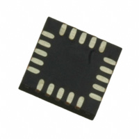
MPR121
Capacitive Touch Sensor Controller
Bottom View
20-PIN QFN CASE 2059-01
Top View
ELE11 ELE10 ELE9 ELE8 15 14 13 12 11 6 VSS 7 REXT 8 ELE0 9 ELE1 10 ELE2 VDD 1 2 3 4 5
20 19 18 17 16 IRQ SCL SDA ADDR VREG ELE7 ELE6 ELE5 ELE4 ELE3
Implementations
Typical Applications
Pin Connections
IRC Address 0x4C - 0x4F
Shipping Tape & Reel
This document contains a product under development. Freescale Semiconductor reserves the right to change or discontinue this product without notice.
© Freescale Semiconductor, Inc., 2009. All rights reserved.
�SCHEMATIC DRAWINGS AND IMPLEMENTATION
VDD 1.71 V to 2.75 V VDD 1.71 V to 2.75 V 0.1 μF 19 18 17 16 15 14 13 12 11 10 9 8
20 6 5 1 2 3 4 7
VDD VSS VREG IRQ SCL SDA ADDR REXT
ELE11/LED7 ELE10/LED6 ELE9/LED5 ELE8/LED4 ELE7/LED3 ELE6/LED2 ELE5/LED1 ELE4/LED0 ELE3 ELE2 ELE1 ELE0 MPR121Q TOUCH SENSOR
75 k 1% GND GND
Figure 1. Configuration 1: MPR121 runs from a 1.71 V to 2.75 V supply.
VDD 2.5 V to 3.6 V VDD 2.5 V to 3.6 V 0.1 μF 19 18 17 16 15 14 13 12 11 10 9 8
20 6 5 1 2 3 4 7
VDD VSS VREG IRQ SCL SDA ADDR REXT
ELE11/LED7 ELE10/LED6 ELE9/LED5 ELE8/LED4 ELE7/LED3 ELE6/LED2 ELE5/LED1 ELE4/LED0 ELE3 ELE2 ELE1 ELE0
0.1 μF 75 k 1% GND GND GND
MPR121Q TOUCH SENSOR
Figure 2. Configuration 2: MPR121 runs from a 2.5 V to 3.6 V supply. Capacitance Sensing The MPR121 uses a constant current touch sensor system with two primary types of control. It can measure capacitances ranging from 10 pF to 2000 pF by varying the current and the amount of time supplied to each electrode. The electrodes are controlled independently allowing for a great deal of flexibility in electrode pattern design. To make setup of the device easier, an automatic configuration system can be used to set the ideal capacitance of each electrode. For information on how to set up this system refer to application note AN3889. Once capacitance is calculated, it runs through a couple of levels of digital filtering allowing for good noise immunity in different environments without sacrificing response time or power consumption. The MPR121 can be configured for sample rates between 1 ms and 128 ms. For information on how to set up this system refer to application note AN3890.
MPR121 2 Sensors Freescale Semiconductor
�Touch Sensing Once the capacitance is determined at any given moment, this information must then be translated into intelligent touch recognition. The MPR121 has a couple of systems that have improved over the previous generation in the MPR03x series devices. A baseline tracking system allows the system to track the untouched capacitance in the system. For information on how to set up the baseline capacitance system refer to application note AN3891. The baseline value is then compared with the current value to determine if a touch has occurred. A designer has the ability to set both the rising and falling thresholds in addition to a debounce to eliminate jitter and false touches due to noise. These elements are described in application note AN3892. Proximity Sensing A new feature of the MPR121 is the use of a proximity sensing system whereby all of a system’s electrodes can be shorted together internally and create a single large electrode. The capacitance of this electrode is larger and projected capacitance can be measured. When enabled, this “13th” electrode will be included at the end of a normal detection cycle and will have its own independent set of configuration registers. This system is described in application note AN3893. LED Driver The MPR121 includes eight shared LED driving pins. When these pins are not configured as electrodes, they may be used to drive LEDs. The system allows for both pull up and pull down LED configurations as well as general GPIO push/pull functionality. The configuration of the LED driver system is described in application note AN3894. Serial Communication The MPR121 is an Inter-Integrated Circuit (I2C) compliant device with an additional interrupt that is triggered any time a touch or release of a button is detected. The device has a configurable I2C address by connecting the ADDR pin to the VDD, VSS, SDA or SCL lines. The resulting I2C addresses are 0x4C, 0x4D, 0x4E and 0x4F respectively. The specific details of this system are described in AN3895. For reference the register map of the MPR121 is included in Table 1.
MPR121 3 Sensors Freescale Semiconductor
�Table 1. Register Map
REGISTER ELE0 - ELE7 Touch Status ELE8 - ELE11, ELEPROX Touch Status ELE0-7 OOR Status ELE8-11, ELEPROX OOR Status ELE0 Electrode Filtered Data LSB ELE0 Electrode Filtered Data MSB ELE1 Electrode Filtered Data LSB ELE1 Electrode Filtered Data MSB ELE2 Electrode Filtered Data LSB ELE2 Electrode Filtered Data MSB ELE3 Electrode Filtered Data LSB ELE3 Electrode Filtered Data MSB ELE4 Electrode Filtered Data LSB ELE4 Electrode Filtered Data MSB ELE5 Electrode Filtered Data LSB ELE5 Electrode Filtered Data MSB ELE6 Electrode Filtered Data LSB ELE6 Electrode Filtered Data MSB ELE7 Electrode Filtered Data LSB ELE7 Electrode Filtered Data MSB ELE8 Electrode Filtered Data LSB ELE8 Electrode Filtered Data MSB ELE9 Electrode Filtered Data LSB ELE9 Electrode Filtered Data MSB ELE10 Electrode Filtered Data LSB ELE10 Electrode Filtered Data MSB ELE11 Electrode Filtered Data LSB ELE11 Electrode Filtered Data MSB ELEPROX Electrode Filtered Data LSB ELEPROX Electrode Filtered Data MSB ELE0 Baseline Value ELE1 Baseline Value ELE2 Baseline Value ELE3 Baseline Value ELE4 Baseline Value ELE5 Baseline Value ELE6 Baseline Value ELE7 Baseline Value ELE8 Baseline Value ELE9 Baseline Value ELE10 Baseline Value ELE11 Baseline Value ELEPROX Baseline Value MHD Rising NHD Amount Rising NCL Rising FDL Rising MHD Falling NHD Amount Falling NCLR FDLR MHDF NHDF E0BV E1BV E2BV E3BV E4BV E5BV E6BV E7BV E8BV E9BV E10BV E11BV EPROXBV MHDR NHDR EFDPROXLB EFDPROXHB EFD11LB EFD11HB EFD10LB EFD10HB EFD9LB EFD9HB EFD8LB EFD8HB EFD7LB EFD7HB EFD6LB EFD6HB EFD5LB EFD5HB EFD4LB EFD4HB EFD3LB EFD3HB EFD2LB EFD2HB EFD1LB EFD1HB ELE7 OVCF ELE7 ARFF ELE6 ELEPROX ELE6 ACFF ELE5 ELE4 ELEPROX ELE5 ELE4 Fields ELE3 ELE11 ELE3 ELE11 ELE2 ELE10 ELE2 ELE10 ELE1 ELE9 ELE1 ELE9 ELE0 ELE8 ELE0 ELE8 Register Address 0x00 0x01 0x02 0x03 0x04 EFD0HB 0x05 0x06 0x07 0x08 0x09 0x0A 0x0B 0x0C 0x0D 0x0E 0x0F 0x10 0x11 0x12 0x13 0x14 0x15 0x16 0x17 0x18 0x19 0x1A 0x1B 0x1C 0x1D 0x1E 0x1F 0x20 0x21 0x22 0x23 0x24 0x25 0x26 0x27 0x28 0x29 0x2A 0x2B 0x2C 0x2D 0x2E 0x2F 0x30 Initial Value 0x00 0x00 0x00 0x00 0x00 0x00 0x00 0x00 0x00 0x00 0x00 0x00 0x00 0x00 0x00 0x00 0x00 0x00 0x00 0x00 0x00 0x00 0x00 0x00 0x00 0x00 0x00 0x00 0x00 0x00 0x00 0x00 0x00 0x00 0x00 0x00 0x00 0x00 0x00 0x00 0x00 0x00 0x00 0x00 0x00 0x00 0x00 0x00 0x00 Register Address + 1 Auto Increment Address
EFD0LB
MPR121 4 Sensors Freescale Semiconductor
�Table 1. Register Map
REGISTER NCL Falling FDL Falling NHD Amount Touched NCL Touched FDL Touched ELEPROX MHD Rising ELEPROX NHD Amount Rising ELEPROX NCL Rising ELEPROX FDL Rising ELEPROX MHD Falling ELEPROX NHD Amount Falling ELEPROX NCL Falling ELEPROX FDL Falling ELEPROX NHD Amount Touched ELEPROX NCL Touched ELEPROX FDL Touched ELE0 Touch Threshold ELE0 Release Threshold ELE1 Touch Threshold ELE1 Release Threshold ELE2 Touch Threshold ELE2 Release Threshold ELE3 Touch Threshold ELE3 Release Threshold ELE4 Touch Threshold ELE4 Release Threshold ELE5 Touch Threshold ELE5 Release Threshold ELE6 Touch Threshold ELE6 Release Threshold ELE7 Touch Threshold ELE7 Release Threshold ELE8 Touch Threshold ELE8 Release Threshold ELE9 Touch Threshold ELE9 Release Threshold ELE10 Touch Threshold ELE10 Release Threshold ELE11 Touch Threshold ELE11 Release Threshold ELEPROX Touch Threshold ELEPROX Release Threshold Debounce Touch & Release AFE Configuration Filter Configuration Electrode Configuration ELE0 Electrode Current ELE1 Electrode Current ELE2 Electrode Current CL FFI CDT EL CDC0 CDC1 CDC2 SFI EleEn DR CDC ESI NCLPROXT FDLPROXT E0TTH E0RTH E1TTH E1RTH E2TTH E2RTH E3TTH E3RTH E4TTH E4RTH E5TTH E5RTH E6TTH E6RTH E7TTH E7RTH E8TTH E8RTH E9TTH E9RTH E10TTH E10RTH E11TTH E11RTH EPROXTTH EPROXRTH DT NCLPROXF FDLPROXF NHDPROXT NCLPROXR FDLPROXR MHDPROXF NHDPROXF NCLT FDLT MHDPROXR NHDPROXR Fields NCLF FDLF NHDT Register Address 0x31 0x32 0x33 0x34 0x35 0x36 0x37 0x38 0x39 0x3A 0x3B 0x3C 0x3D 0x3E 0x3F 0x40 0x41 0x42 0x43 0x44 0x45 0x46 0x47 0x48 0x49 0x4A 0x4B 0x4C 0x4D 0x4E 0x4F 0x50 0x51 0x52 0x53 0x54 0x55 0x56 0x57 0x58 0x59 0x5A 0x5B 0x5C 0x5D 0x5E 0x5F 0x60 0x61 Initial Value 0x00 0x00 0x00 0x00 0x00 0x00 0x00 0x00 0x00 0x00 0x00 0x00 0x00 0x00 0x00 0x00 0x00 0x00 0x00 0x00 0x00 0x00 0x00 0x00 0x00 0x00 0x00 0x00 0x00 0x00 0x00 0x00 0x00 0x00 0x00 0x00 0x00 0x00 0x00 0x00 0x00 0x00 0x00 0x10 0x04 0x00 0x00 0x00 0x00 Register Address + 1 Auto Increment Address
MPR121 Sensors Freescale Semiconductor 5
�Table 1. Register Map
REGISTER ELE3 Electrode Current ELE4 Electrode Current ELE5 Electrode Current ELE6 Electrode Current ELE7 Electrode Current ELE8 Electrode Current ELE9 Electrode Current ELE10 Electrode Current ELE11 Electrode Current ELEPROX Electrode Current ELE0, ELE1 Charge Time ELE2, ELE3 Charge Time ELE4, ELE5 Charge Time ELE6, ELE7 Charge Time ELE8, ELE9 Charge Time ELE10, ELE11 Charge Time ELEPROX Charge Time GPIO Control Register 0 GPIO Control Register 1 GPIO Data Register GPIO Direction Register GPIO Enable Register GPIO Data Set Register GPIO Data Clear Register GPIO Data Toggle Register AUTO-CONFIG Control Register 0 AUTO-CONFIG Control Register 1 AUTO-CONFIG USL Register AUTO-CONFIG LSL Register AUTO-CONFIG Target Level Register SCTS USL LSL TL CTL011 CTL111 DAT11 DIR11 EN11 SET11 CLR11 TOG11 AFES CTL010 CTL110 DAT10 DIR10 EN10 SET10 CLR10 TOG10 CTL09 CTL19 DAT9 DIR9 EN9 SET9 CLR9 TOG9 CTL08 CTL18 DAT8 DIR8 EN8 SET8 CLR8 TOG8 CTL07 CTL17 DAT7 DIR7 EN7 SET7 7CLR7 TOG7 BVA OORIE CTL06 CTL16 DAT6 DIR6 EN6 SET6 CLR6 TOG6 CDT1 CDT3 CDT5 CDT7 CDT9 CDT11 CDC3 CDC4 CDC5 CDC6 CDC7 CDC8 CDC9 CDC10 CDC11 CDCPROX CDT0 CDT2 CDT4 CDT6 CDT8 CDT10 CDTPROX CTL05 CTL15 DAT5 DIR5 EN5 SET5 CLR5 TOG5 ARE ARFIE CTL04 CTL14 DAT4 DIR4 EN4 SET4 CLR4 TOG4 ACE ACFIE Fields Register Address 0x62 0x63 0x64 0x65 0x66 0x67 0x68 0x69 0x6A 0x6B 0x6C 0x6D 0x6E 0x6F 0x70 0x71 0x72 0x73 0x74 30x75 0x76 0x77 0x78 0x79 0x7A 0x7B 0x7C 0x7D 0x7E 0x7F Initial Value 0x00 0x00 0x00 0x00 0x00 0x00 0x00 0x00 0x00 0x00 0x00 0x00 0x00 0x00 0x00 0x00 0x00 0x00 0x00 0x00 0x00 0x00 0x00 0x00 0x00 0x00 0x00 0x00 0x00 0x00 0x00 Register Address + 1 Auto Increment Address
RETRY
MPR121 6 Sensors Freescale Semiconductor
�ELECTRICAL CHARACTERISTICS
Absolute Maximum Ratings Absolute maximum ratings are stress ratings only, and functional operation at the maxima is not guaranteed. Stress beyond the limits specified in Table 2 may affect device reliability or cause permanent damage to the device. For functional operating conditions, refer to the remaining tables in this section. This device contains circuitry protecting against damage due to high static voltage or electrical fields; however, it is advised that normal precautions be taken to avoid application of any voltages higher than maximum-rated voltages to this high-impedance circuit. Table 2. Absolute Maximum Ratings - Voltage (with respect to VSS)
Rating Supply Voltage Supply Voltage Input Voltage Symbol VDD VREG VIN TO iGPIO iGPIO TS Value -0.3 to +3.6 -0.3 to +2.75 VSS - 0.3 to VDD + 0.3 -40 to +85 12 1.2 -40 to +125 Unit V V V °C mA mA °C
SCL, SDA, IRQ
Operating Temperature Range GPIO Source Current per Pin GPIO Sink Current per Pin Storage Temperature Range
ESD AND LATCH-UP PROTECTION CHARACTERISTICS
Normal handling precautions should be used to avoid exposure to static discharge. Qualification tests are performed to ensure that these devices can withstand exposure to reasonable levels of static without suffering any permanent damage. During the device qualification ESD stresses were performed for the Human Body Model (HBM), the Machine Model (MM) and the Charge Device Model (CDM). A device is defined as a failure if after exposure to ESD pulses the device no longer meets the device specification. Complete DC parametric and functional testing is performed per the applicable device specification at room temperature followed by hot temperature, unless specified otherwise in the device specification. Table 3. ESD and Latch-up Test Conditions
Rating Human Body Model (HBM) Machine Model (MM) Charge Device Model (CDM) Latch-up current at TA = 85°C Symbol VESD VESD VESD ILATCH Value ±2000 ±200 ±500 ±100 Unit V V V mA
MPR121 Sensors Freescale Semiconductor 7
�DC CHARACTERISTICS
This section includes information about power supply requirements and I/O pin characteristics. Table 4. DC Characteristics (Typical Operating Circuit, VDD and VREG = 1.8 V, TA = 25°C, unless otherwise noted.)
Parameter High Supply Voltage Low Supply Voltage Average Supply Current Average Supply Current Average Supply Current Average Supply Current Average Supply Current Average Supply Current Average Supply Current Average Supply Current Measurement Supply Current Idle Supply Current Input Leakage Current ELE_ Input Capacitance ELE_ Input High Voltage SDA, SCL Input Low Voltage SDA, SCL Input Leakage Current SDA, SCL Input Capacitance SDA, SCL Output Low Voltage SDA, IRQ Output High Voltage ELE4 - ELE11 (GPIO mode) Output Low Voltage ELE4 - ELE11 (GPIO mode) Power On Reset VOL VOHGPIO IOL = 6mA VDD = 2.7 V to 3.6 V: IOHGPIO = -10 mA VDD = 2.3 V to 2.7 V: IOHGPIO = -6 mA VDD = 1.8 V to 2.3 V: IOHGPIO = -3 mA IOLGPIOD = 1 mA VDD rising VDD falling 1.08 0.88 1.35 1.15 VDD - 0.5 VIH VIL IIH, IIL 0.025 0.7 x VDD 0.3 x VDD 1 7 0.5V Symbol VDD VREG IDD IDD IDD IDD IDD IDD IDD IDD IDD IDD IIH, IIL Run1 Mode @ 1 ms sample period Run1 Mode @ 2 ms sample period Run1 Mode @ 4 ms sample period Run1 Mode @ 8 ms sample period Run1 Mode @ 16 ms sample period Run1 Mode @ 32 ms sample period Run1 Mode @ 64 ms sample period Run1 Mode @ 128 ms sample period Peak of measurement duty cycle Stop Mode Conditions Min 2.5 1.71 Typ 3.3 1.8 393 199 102 54 29 17 11 8 1 3 0.025 15 Max 3.6 2.75 Units V V μA μA μA μA μA μA μA μA mA μA μA pF V V μA pF V V
VOLGPIO VTLH VTHL
0.5 1.62 1.42
V V V
AC CHARACTERISTICS
Table 5. AC CHARACTERISTICS
(Typical Operating Circuit, VDD and VREG = 1.8 V, TA = 25°C, unless otherwise noted.)
Parameter 8 MHz Internal Oscillator 1 kHz Internal Oscillator Symbol fH fL Conditions Min 7.44 0.65 Typ 8 1 Max 8.56 1.35 Units MHz kHz
MPR121 8 Sensors Freescale Semiconductor
�I2C AC CHARACTERISTICS
Table 6. I2C AC Characteristics
(Typical Operating Circuit, VDD and VREG = 1.8 V, TA = 25°C, unless otherwise noted.)
Parameter Serial Clock Frequency Bus Free Time Between a STOP and a START Condition Hold Time, (Repeated) START Condition Repeated START Condition Setup Time STOP Condition Setup Time Data Hold Time Data Setup Time SCL Clock Low Period SCL Clock High Period Rise Time of Both SDA and SCL Signals, Receiving Fall Time of Both SDA and SCL Signals, Receiving Fall Time of SDA Transmitting Pulse Width of Spike Suppressed Capacitive Load for Each Bus Line Symbol fSCL tBUF tHD, STA tSU, STA tSU, STO tHD, DAT tSU, DAT tLOW tHIGH tR tF tF.TX tSP Cb 100 1.3 0.7 20+0.1Cb 20+0.1Cb 20+0.1Cb 25 400 300 300 250 1.3 0.6 0.6 0.6 0.9 Conditions Min Typ Max 400 Units kHz μs μs μs μs μs ns μs μs ns ns ns ns pF
MPR121 Sensors Freescale Semiconductor 9
�PACKAGE DIMENSIONS
PAGE 1 OF 3
MPR121 10 Sensors Freescale Semiconductor
�PAGE 2 OF 3
MPR121 Sensors Freescale Semiconductor 11
�PACKAGE DIMENSIONS
PAGE 3 OF 3
MPR121 12 Sensors Freescale Semiconductor
�How to Reach Us:
Home Page: www.freescale.com Web Support: http://www.freescale.com/support USA/Europe or Locations Not Listed: Freescale Semiconductor, Inc. Technical Information Center, EL516 2100 East Elliot Road Tempe, Arizona 85284 1-800-521-6274 or +1-480-768-2130 www.freescale.com/support Europe, Middle East, and Africa: Freescale Halbleiter Deutschland GmbH Technical Information Center Schatzbogen 7 81829 Muenchen, Germany +44 1296 380 456 (English) +46 8 52200080 (English) +49 89 92103 559 (German) +33 1 69 35 48 48 (French) www.freescale.com/support Japan: Freescale Semiconductor Japan Ltd. Headquarters ARCO Tower 15F 1-8-1, Shimo-Meguro, Meguro-ku, Tokyo 153-0064 Japan 0120 191014 or +81 3 5437 9125 support.japan@freescale.com Asia/Pacific: Freescale Semiconductor China Ltd. Exchange Building 23F No. 118 Jianguo Road Chaoyang District Beijing 100022 China +86 010 5879 8000 support.asia@freescale.com For Literature Requests Only: Freescale Semiconductor Literature Distribution Center 1-800-441-2447 or +1-303-675-2140 Fax: +1-303-675-2150 LDCForFreescaleSemiconductor@hibbertgroup.com
Information in this document is provided solely to enable system and software implementers to use Freescale Semiconductor products. There are no express or implied copyright licenses granted hereunder to design or fabricate any integrated circuits or integrated circuits based on the information in this document. Freescale Semiconductor reserves the right to make changes without further notice to any products herein. Freescale Semiconductor makes no warranty, representation or guarantee regarding the suitability of its products for any particular purpose, nor does Freescale Semiconductor assume any liability arising out of the application or use of any product or circuit, and specifically disclaims any and all liability, including without limitation consequential or incidental damages. “Typical” parameters that may be provided in Freescale Semiconductor data sheets and/or specifications can and do vary in different applications and actual performance may vary over time. All operating parameters, including “Typicals”, must be validated for each customer application by customer’s technical experts. Freescale Semiconductor does not convey any license under its patent rights nor the rights of others. Freescale Semiconductor products are not designed, intended, or authorized for use as components in systems intended for surgical implant into the body, or other applications intended to support or sustain life, or for any other application in which the failure of the Freescale Semiconductor product could create a situation where personal injury or death may occur. Should Buyer purchase or use Freescale Semiconductor products for any such unintended or unauthorized application, Buyer shall indemnify and hold Freescale Semiconductor and its officers, employees, subsidiaries, affiliates, and distributors harmless against all claims, costs, damages, and expenses, and reasonable attorney fees arising out of, directly or indirectly, any claim of personal injury or death associated with such unintended or unauthorized use, even if such claim alleges that Freescale Semiconductor was negligent regarding the design or manufacture of the part. Freescale™ and the Freescale logo are trademarks of Freescale Semiconductor, Inc. All other product or service names are the property of their respective owners. © Freescale Semiconductor, Inc. 2009. All rights reserved.
RoHS-compliant and/or Pb-free versions of Freescale products have the functionality and electrical characteristics of their non-RoHS-compliant and/or non-Pb-free counterparts. For further information, see http:/www.freescale.com or contact your Freescale sales representative. For information on Freescale’s Environmental Products program, go to http://www.freescale.com/epp. MPR121 Rev. 0 9/2009
�