Freescale Semiconductor Technical Data
Document Number: MW4IC2230N Rev. 6, 5/2006
RF LDMOS Wideband Integrated Power Amplifiers
The MW4IC2230N wideband integrated circuit is designed for W - CDMA base station applications. It uses Freescale’s newest High Voltage (26 to 28 Volts) LDMOS IC technology and integrates a multi - stage structure. Its wideband on- chip design makes it usable from 1600 to 2400 MHz. The linearity performances cover all modulations for cellular applications: GSM, GSM EDGE, TDMA, CDMA and W - CDMA. Final Application • Typical Single - Carrier W - CDMA Performance: VDD = 28 Volts, IDQ1 = 60 mA, IDQ2 = 350 mA, Pout = 5 Watts Avg., f = 2140 MHz, Channel Bandwidth = 3.84 MHz, PAR = 8.5 dB @ 0.01% Probability on CCDF. Power Gain — 31 dB Drain Efficiency — 15% ACPR @ 5 MHz = - 45 dBc in 3.84 MHz Bandwidth Driver Application • Typical Single - Carrier W - CDMA Performance: VDD = 28 Volts, IDQ1 = 60 mA, IDQ2 = 350 mA, Pout = 0.4 Watts Avg., f = 2140 MHz, Channel Bandwidth = 3.84 MHz, PAR = 8.5 dB @ 0.01% Probability on CCDF. Power Gain — 31.5 dB ACPR @ 5 MHz = - 53.5 dBc in 3.84 MHz Bandwidth • Capable of Handling 3:1 VSWR, @ 28 Vdc, 2170 MHz, 5 Watts CW Output Power • Stable into a 3:1 VSWR. All Spurs Below - 60 dBc @ 10 mW to 5 W CW Pout. Features • Characterized with Series Equivalent Large - Signal Impedance Parameters • On - Chip Matching (50 Ohm Input, DC Blocked, >5 Ohm Output) • Integrated Quiescent Current Temperature Compensation with Enable/Disable Function • On - Chip Current Mirror gm Reference FET for Self Biasing Application (1) • Integrated ESD Protection • 200°C Capable Plastic Package • N Suffix Indicates Lead - Free Terminations. RoHS Compliant. • In Tape and Reel. R1 Suffix = 500 Units per 44 mm, 13 inch Reel
MW4IC2230NBR1 MW4IC2230GNBR1
2110 - 2170 MHz, 30 W, 28 V SINGLE W - CDMA RF LDMOS WIDEBAND INTEGRATED POWER AMPLIFIERS
CASE 1329 - 09 TO - 272 WB - 16 PLASTIC MW4IC2230NBR1
CASE 1329A - 03 TO - 272 WB - 16 GULL PLASTIC MW4IC2230GNBR1
VRD1 VRG1 VDS2 VDS1
GND VDS2 VRD1 VRG1 VDS1 3 Stages IC RFin
1 2 3 4 5 6 7 8 9 10 11
16 15
GND
14
VDS3/ RFout
RFin
VDS3/RFout
VGS1 VGS2 VGS3
VGS1 VGS2 VGS3 GND
13 12 (Top View)
GND
Quiescent Current Temperature Compensation
Note: Exposed backside flag is source terminal for transistors.
Figure 1. Functional Block Diagram
Figure 2. Pin Connections
1. Refer to AN1987, Quiescent Current Control for the RF Integrated Circuit Device Family. Go to http://www.freescale.com/rf. Select Documentation/Application Notes - AN1987.
© Freescale Semiconductor, Inc., 2006. All rights reserved.
MW4IC2230NBR1 MW4IC2230GNBR1 1
RF Device Data Freescale Semiconductor
�Table 1. Maximum Ratings
Rating Drain- Source Voltage Gate- Source Voltage Storage Temperature Range Operating Channel Temperature Input Power Symbol VDSS VGS Tstg TJ Pin Value - 0.5, +65 - 0.5, +8 - 65 to +175 200 20 Unit Vdc Vdc °C °C dBm
Table 2. Thermal Characteristics
Characteristic Thermal Resistance, Junction to Case Stage 1 Stage 2 Stage 3 Symbol RθJC Value (1) 10.5 5.1 2.3 Unit °C/W
Table 3. ESD Protection Characteristics
Test Conditions Human Body Model Machine Model Charge Device Model Class 2 (Minimum) M3 (Minimum) C5 (Minimum)
Table 4. Moisture Sensitivity Level
Test Methodology Per JESD 22 - A113, IPC/JEDEC J - STD - 020 Rating 3 Package Peak Temperature 260 Unit °C
Table 5. Electrical Characteristics (TC = 25°C unless otherwise noted)
Characteristic Symbol Min Typ Max Unit Functional Tests (In Freescale Test Fixture, 50 ohm system) VDD = 28 Vdc, IDQ1 = 60 mA, IDQ2 = 350 mA, IDQ3 = 265 mA, Pout = 0.4 W Avg., f = 2110 MHz, f = 2170 MHz, Single - carrier W - CDMA. ACPR measured in 3.84 MHz Channel Bandwidth @ ±5 MHz Offset. PAR = 8.5 dB @ 0.01% Probability on CCDF. Power Gain Input Return Loss Adjacent Channel Power Ratio Pout = 0.4 W Avg. Pout = 1.26 W Avg. Gps IRL ACPR — — - 53.5 - 52 - 50 — 29 — 31.5 - 25 — - 10 dB dB dBc
Typical Performances (In Freescale Test Fixture tuned for 0.4 W Avg. W - CDMA driver) VDD = 28 Vdc, IDQ1 = 60 mA, IDQ2 = 350 mA, IDQ3 = 265 mA, 2110 MHz
很抱歉,暂时无法提供与“MW4IC2230NBR1”相匹配的价格&库存,您可以联系我们找货
免费人工找货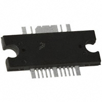


 工商网监
湘ICP备2023018690号
工商网监
湘ICP备2023018690号
