EVAL232R FT232RL USB to RS232 Evaluation Module Datasheet
Version 1.0
Document No.: FT_001424 Clearance No.: FTDI#544
Future Technology Devices
International Ltd
EVAL232R
FT232RL USB to RS232 Evaluation
Module
Datasheet
Neither the whole nor any part of the information contained in, or the product described in this manual, may be adapted or reproduced in
any material or electronic form without the prior written consent of the copyright holder. This product and its documentation are supplied
on an as-is basis and no warranty as to their suitability for any particular purpose is either made or implied. Future Technology Devices
International Ltd will not accept any claim for damages howsoever arising as a result of use or failure of this product. Your statutory rights
are not affected. This product or any variant of it is not intended for use in any medical appliance, device or system in which the failure of
the product might reasonably be expected to result in personal injury. This document provides preliminary information that may be
subject to change without notice. No freedom to use patents or other intellectual property rights is implied by the publication of this
document. Future Technology Devices International Ltd, Unit 1, 2 Seaward Place, Centurion Business Park, Glasgow, G41 1HH, United
Kingdom. Scotland Registered Number: SC136640
Copyright © Future Technology Devices International Limited
1
�EVAL232R FT232RL USB to RS232 Evaluation Module Datasheet
Version 1.0
Document No.: FT_001424 Clearance No.: FTDI#544
Table of Contents
1
Introduction .................................................................... 4
2
Typical Applications ........................................................ 5
2.1
Driver Support .......................................................................... 5
2.2
Features .................................................................................... 6
3
FT232RQ Features and Enhancements ............................ 7
4
EVAL232R Pin Out and Signal Descriptions ................... 10
4.1
EVAL232R Pin Out ................................................................... 10
4.2
Signal Descriptions ................................................................. 11
4.3
CBUS Signal Options ............................................................... 12
4.4
RS232 Signal Descriptions ...................................................... 13
5
Module Dimensions ....................................................... 14
6
Device Characteristics and Ratings ............................... 15
7
6.1
Absolute Maximum Ratings ..................................................... 15
6.2
DC Characteristics ................................................................... 15
6.3
EEPROM Reliability Characteristics ......................................... 17
6.4
Internal Clock Characteristics ................................................. 17
Module Configurations .................................................. 18
7.1
BUS Powered Configuration .................................................... 18
7.2
Self Powered Configuration .................................................... 18
7.3
USB Bus Powered with Power Switching Configuration .......... 18
7.4
LED Interface .......................................................................... 19
8
EVAL232R Module Circuit Schematic ............................. 20
9
Internal EEPROM Configuration..................................... 22
10 Contact Information ...................................................... 24
Appendix A – References ................................................... 25
Document References ..................................................................... 25
Acronyms and Abbreviations ........................................................... 25
Appendix B – List of Tables and Figures ............................. 26
List of Tables ................................................................................... 26
List of Figures ................................................................................. 26
Copyright © Future Technology Devices International Limited
2
�EVAL232R FT232RL USB to RS232 Evaluation Module Datasheet
Version 1.0
Document No.: FT_001424 Clearance No.: FTDI#544
Appendix C – Revision History ........................................... 27
Copyright © Future Technology Devices International Limited
3
�EVAL232R FT232RL USB to RS232 Evaluation Module Datasheet
Version 1.0
Document No.: FT_001424 Clearance No.: FTDI#544
1 Introduction
The EVAL232R is a USB to RS232 evaluation module for FTDI’s FT232RL USB - Serial UART interface IC
device.
The FT232RL is a USB to serial UART interface with optional clock generator output, and the FTDIChip-ID™
security dongle feature. In addition, asynchronous and synchronous bit bang interface modes are available.
USB to serial interface designs using the FT232RL have been further simplified by fully integrating the
external EEPROM, clock circuit and USB resistors onto the device.
The FT232RL adds two new functions compared with its predecessors, effectively making it a “3-in-1” chip
for some application areas. The internally generated clock (6MHz, 12MHz, 24MHz, and 48MHz) can be
brought out of the device and used to drive a microcontroller or external logic. A unique number (the
FTDIChip-ID™) is burnt into the device during manufacture and is readable over USB, thus forming the basis
of a security dongle which can be used to protect customer application software from being copied.
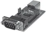
The EVAL232R is supplied on a 61.0mm x 32.0mm (2.40” x 1.26”) PCB. All components used, including the
FT232RL and RS232 level converter IC are Pb-free (RoHS compliant).
Figure 1.1 – EVAL232R FT232RL USB to RS232 Evaluation Module
Copyright © Future Technology Devices International Limited
4
�EVAL232R FT232RL USB to RS232 Evaluation Module Datasheet
Version 1.0
Document No.: FT_001424 Clearance No.: FTDI#544
2 Typical Applications
USB to RS232 Converter
Upgrading Legacy Peripherals to USB
USB Audio and Low Bandwidth Video data transfer
PDA to USB data transfer
USB Smart Card Readers
USB Instrumentation
USB Industrial Control
USB MP3 Player Interface
USB FLASH Card Reader / Writers
Set Top Box PC - USB interface
USB Digital Camera Interface
USB Hardware Modems
USB Wireless Modems
USB Bar Code Readers
USB Software / Hardware Encryption Dongles
2.1 Driver Support
Royalty free VIRTUAL COM PORT
(VCP) DRIVERS for...
Royalty free D2XX Direct Drivers
(USB Drivers + DLL S/W Interface)
Windows 10 32,64-bit
Windows 10 32,64-bit
Windows 8/8.1 32,64-bit
Windows 8/8.1 32,64-bit
Windows 7 32,64-bit
Windows 7 32,64-bit
Windows Vista and Vista 64-bit
Windows Vista and Vista 64-bit
Windows XP and XP 64-bit
Windows XP and XP 64-bit
Windows 98, 98SE, ME, 2000, Server 2003, XP,
Server 2008 and server 2012 R2
Windows 98, 98SE, ME, 2000, Server 2003, XP,
Server 2008 and server 2012 R2
Windows XP Embedded
Windows XP Embedded
Windows CE 4.2, 5.0 and 6.0
Windows CE 4.2, 5.0 and 6.0
Mac OS 8/9, OS-X
Linux 2.4 and greater
Linux 2.4 and greater
Android(J2xx)
The drivers listed above are all available to download for free from FTDI website (www.ftdichip.com).
Various 3rd party drivers are also available for other operating systems - see FTDI website
(www.ftdichip.com) for details.
For driver installation, please refer to http://www.ftdichip.com/Documents/InstallGuides.htm
Copyright © Future Technology Devices International Limited
5
�EVAL232R FT232RL USB to RS232 Evaluation Module Datasheet
Version 1.0
Document No.: FT_001424 Clearance No.: FTDI#544
2.2 Features
The EVAL232R has the following features:
FT232RL provides single chip USB to
asynchronous serial data transfer interface.
Module provides USB to RS232 interface,
with additional I/O pinout.
Device supplied pre-programmed
unique USB serial number.
Support for USB suspend and resume.
Module supply voltage comes from VCC – no
external supply required.
5V USB power available to supply external
devices.
Integrated 3.3V level converter for USB I/O
Entire USB protocol handled on the FT232RL
chip
No
USB-specific
firmware
programming required.
UART interface support for 7 or 8 data bits,
1 or 2 stop bits and odd / even / mark /
space / no parity.
with
Fully assisted hardware or X-On / X-Off
software handshaking.
Integrated level converter on UART and
CBUS for interfacing to 5V - 1.8V Logic.
Data transfer rates from 300 baud to 1
Megabaud at RS232 levels.
On board jumper allows for selection of
UART and CBUS interface IO voltage.
FTDI’s royalty-free VCP and D2XX drivers
eliminate the requirement for USB driver
development in most cases.
True 5V / 3.3V / 2.8V / 1.8V CMOS drive
output and TTL input.
High I/O pin output drive option.
In-built support for event characters and
line break condition.
Integrated USB resistors.
New USB FTDIChip-ID™ feature.
Integrated power-on-reset circuit.
New configurable CBUS I/O pins.
Fully integrated clock - no external crystal,
oscillator, or resonator required.
Transmit and receive LED’s to indicate serial
data transfer.
New 48MHz, 24MHz, 12MHz, and 6MHz
clock output signal Options.
Fully integrated AVCC supply filtering - No
separate AVCC pin and no external R-C filter
required.
USB bulk transfer mode.
Low operating and USB suspend current.
Low USB bandwidth consumption.
UHCI / OHCI
compatible
USB 2.0 Full Speed compatible.
-40°C
to
85°C
temperature range.
Supplied on miniature 61.0mm x 32.0mm
(2.40” x 1.26”) PCB with 15 board header
pins.
Connect to a PC via a standard USB A to B
USB cable.
FIFO receive and transmit buffers for high
data throughput.
Adjustable receive buffer timeout.
Synchronous and asynchronous bit bang
mode interface options with RD# and WR#
strobes.
New CBUS bit bang mode option.
Integrated 1024 bit internal EEPROM for
storing USB VID, PID, serial number and
product description strings, and CBUS I/O
configuration.
Copyright © Future Technology Devices International Limited
/
EHCI
host
extended
controller
operating
6
�EVAL232R FT232RL USB to RS232 Evaluation Module Datasheet
Version 1.0
Document No.: FT_001424 Clearance No.: FTDI#544
3 FT232RQ Features and Enhancements
Key Features
This section summarises the key features and enhancements of the FT232RL IC device which is used on the
EVAL232R Module. For further details, consult the FT232R datasheet, which is available from
www.ftdichip.com.
Integrated Clock Circuit - Previous generations of FTDI’s USB UART devices required an external crystal
or ceramic resonator. The clock circuit has now been integrated onto the device meaning that no crystal or
ceramic resonator is required. However, if preferred, an external 12MHz crystal can be used as the clock
source.
Integrated EEPROM - Previous generations of FTDI’s USB UART devices required an external EEPROM if
the device were to use USB Vendor ID (VID), Product ID (PID), serial number and product description
strings other than the default values in the device itself. This external EEPROM has now been integrated
onto the FT232R chip meaning that all designs have the option to change the product description strings. A
user area of the internal EEPROM is available for storing additional data. The internal EEPROM is
programmable in circuit, over USB without any additional voltage requirement.
Preprogrammed EEPROM - The FT232R is supplied with its internal EEPROM pre-programmed with a
serial number which is unique to each individual device. This, in most cases, will remove the need to
program the device EEPROM.
Integrated USB Resistors - Previous generations of FTDI’s USB UART devices required two external
series resistors on the USBDP and USBDM lines, and a 1.5 kΩ pull up resistor on USBDP. These three
resistors have now been integrated onto the device.
Integrated AVCC Filtering - Previous generations of FTDI’s USB UART devices had a separate AVCC pin –
the supply to the internal PLL. This pin required an external R-C filter. The separate AVCC pin is now
connected internally to VCC, and the filter has now been integrated onto the chip.
Less External Components - Integration of the crystal, EEPROM, USB resistors, and AVCC filter will
substantially reduce the bill of materials cost for USB interface designs using the FT232R compared to its
FT232BM predecessor.
Configurable CBUS I/O Pin Options - There are now 5 configurable Control Bus (CBUS) lines. Options
are TXDEN - transmit enable for RS485 designs, PWREN# - Power control for high power, bus powered
designs, TXLED# - for pulsing an LED upon transmission of data, RXLED# - for pulsing an LED upon
receiving data, TX&RXLED# - which will pulse an LED upon transmission OR reception of data, SLEEP# indicates that the device going into USB suspend mode, CLK48 / CLK24 / CLK12 / CLK6 - 48MHz,
24MHz,12MHz, and 6MHz clock output signal options. There is also the option to bring out bit bang mode
read and write strobes (see below). The CBUS lines can be configured with any one of these output options
by setting bits in the internal EEPROM. The device is supplied with the most commonly used pin definitions
pre-programmed - see Section 9 for details.
Enhanced Asynchronous Bit Bang Mode with RD# and WR# Strobes - The FT232R supports FTDI’s
BM chip bit bang mode. In bit bang mode, the eight UART lines can be switched from the regular interface
mode to an 8-bit general purpose I/O port. Data packets can be sent to the device and they will be
sequentially sent to the interface at a rate controlled by an internal timer (equivalent to the baud rate
prescaler). With the FT232R device this mode has been enhanced so that the internal RD# and WR#
strobes are now brought out of the device which can be used to allow external logic to be clocked by
accesses to the bit bang I/O bus. This option will be described more fully in a separate application note.
Synchronous Bit Bang Mode - Synchronous bit bang mode differs from asynchronous bit bang mode in
that the interface pins are only read when the device is written to. Thus making it easier for the controlling
program to measure the response to an output stimulus as the data returned is synchronous to the output
data. The feature was previously seen in FTDI’s FT2232C device. This option will be described more fully in
a separate application note.
CBUS Bit Bang Mode - This mode allows four of the CBUS pins to be individually configured as GPIO pins,
similar to Asynchronous bit bang mode. It is possible to use this mode while the UART interface is being
Copyright © Future Technology Devices International Limited
7
�EVAL232R FT232RL USB to RS232 Evaluation Module Datasheet
Version 1.0
Document No.: FT_001424 Clearance No.: FTDI#544
used, thus providing up to four general purpose I/O pins which are available during normal operation. An
application note describing this feature is available separately from www.ftdichip.com.
Lower Supply Voltage - Previous generations of the chip required 5V supply on the VCC pin. The FT232R
will work with a VCC supply in the range 3.5V to 5.25V. Bus powered designs would still take their supply
from the 5V on the USB bus, but for self-powered designs where only 3.5V is available and there is no 5V
supply there is no longer any need for an additional external regulator.
Integrated Level Converter on UART Interface and Control Signals - VCCIO pin supply can be from
1.8V to 5V. Connecting the VCCIO pin to 1.8V, 2.8V, or 3.3V allows the device to directly interface to 1.8V,
2.8V or 3.3V and other logic families without the need for external level converter I.C. devices.
5V / 3.3V / 2.8V / 1.8V Logic Interface - The FT232R provides true CMOS Drive Outputs and TTL level
Inputs.
Integrated Power-On-Reset (POR) Circuit- The device incorporates an internal POR function. A RESET#
pin is available in order to allow external logic to reset the FT232R where required. However, for many
applications the RESET# pin can be left unconnected, or pulled up to VCCIO.
Lower Operating and Suspend Current - The device operating supply current has been further reduced
to 15mA, and the suspend current has been reduced to around 70μA. This allows greater margin for
peripheral designs to meet the USB suspend current limit of 500μA.
Low USB Bandwidth Consumption - The operation of the USB interface to the FT232R has been
designed to use as little as possible of the total USB bandwidth available from the USB host controller.
High Output Drive Option - The UART interface and CBUS I/O pins can be made to drive out at three
times the standard signal drive level thus allowing multiple devices to be driven, or devices that require
greater signal drive strength to be interfaced to the FT232R. This option is enabled in the internal EEPROM.
Power Management Control for USB Bus Powered, High Current Designs - The PWREN# signal can
be used to directly drive a transistor or P-Channel MOSFET in applications where power switching of
external circuitry is required. An option in the internal EEPROM makes the device gently pull down on its
UART interface lines when the power is shut off (PWREN# is high). In this mode any residual voltage on
external circuitry is bled to GND when power is removed, thus ensuring that external circuitry controlled by
PWREN# resets reliably when power is restored.
UART Pin Signal Inversion - The sense of each of the eight UART signals can be individually inverted by
setting options in the internal EEPROM. Thus, CTS# (active low) can be changed to CTS (active high), or
TXD can be changed to TXD#.
FTDIChip-ID™ - Each FT232R is assigned a unique number which is burnt into the device at manufacture.
This ID number cannot be reprogrammed by product manufacturers or end-users. This allows the possibility
of using FT232R based dongles for software licensing. Further to this, a renewable license scheme can be
implemented based on the FTDIChip-ID™ number when encrypted with other information. This encrypted
number can be stored in the user area of the FT232R internal EEPROM, and can be decrypted, then
compared with the protected FTDIChip-ID™ to verify that a license is valid. Web based applications can be
used to maintain product licensing this way. An application note describing this feature is available
separately from www.ftdichip.com.
Improved EMI Performance - The reduced operating current and improved on-chip VCC decoupling
significantly improves the ease of PCB design requirements in order to meet FCC, CE and other EMI related
specifications.
Programmable Receive Buffer Timeout - The receive buffer timeout is used to flush remaining data
from the receive buffer. This time defaults to 16ms, but is programmable over USB in 1ms increments from
1ms to 255ms, thus allowing the device to be optimised for protocols that require fast response times from
short data packets.
Baud Rates - The FT232R supports all standard baud rates and non-standard baud rates from 300 Baud up
to 3 Megabaud. Achievable non-standard baud rates are calculated as follows -Baud Rate = 3000000 / (n +
x) where ‘n’ can be any integer between 2 and 16,384 (= 2 14 ) and ‘x’ can be a sub-integer of the value 0,
0.125, 0.25, 0.375, 0.5, 0.625, 0.75, or 0.875. When n = 1, x = 0, i.e. baud rate divisors with values
between 1 and 2 are not possible. This gives achievable baud rates in the range 183.1 baud to 3,000,000
Copyright © Future Technology Devices International Limited
8
�EVAL232R FT232RL USB to RS232 Evaluation Module Datasheet
Version 1.0
Document No.: FT_001424 Clearance No.: FTDI#544
baud. When a non-standard baud rate is required simply pass the required baud rate value to the driver as
normal, and the FTDI driver will calculate the required divisor, and set the baud rate. See FTDI application
note AN232B-05 for more details.
Extended Operating Temperature Range - The FT232R operates over an extended temperature range
of -40º to +85º C thus allowing the device to be used in automotive and industrial applications.
New Package Options - The FT232R is available in two packages - a compact 28 pin SSOP (FT232RL) and
an ultra-compact 5mm x 5mm pinless QFN-32 package (FT232RQ). Both packages are lead ( Pb ) free, and
use a ‘green’ compound. Both packages are fully compliant with European Union directive 2002/95/EC. The
EVAL232R module uses a FT232RL device in its design.
Copyright © Future Technology Devices International Limited
9
�EVAL232R FT232RL USB to RS232 Evaluation Module Datasheet
Version 1.0
Document No.: FT_001424 Clearance No.: FTDI#544
4 EVAL232R Pin Out and Signal Descriptions
4.1 EVAL232R Pin Out
Figure 4.1 Module Pin Out
Figure 4.2 EVAL232R RS232 (DB9) Pin Out
Copyright © Future Technology Devices International Limited
10
�EVAL232R FT232RL USB to RS232 Evaluation Module Datasheet
Version 1.0
Document No.: FT_001424 Clearance No.: FTDI#544
4.2 Signal Descriptions
Pin
No.
Name
Type
Description
1
VCC
Output
5V Power output USB port. For a low power USB bus powered design, up to
100mA can be sourced from the 5V supply on the USB bus. A maximum of
500mA can be sourced from the USB bus in a high power USB bus powered
design.
2
VCCIO
Input
+1.8V to +5.25V supply to the FT232RL’s UART Interface and CBUS I/O pins.
In USB bus powered designs connect to 3V3 to drive out at 3.3V levels
(connect VCCIO to VCC3O), or connect to VCC to drive out at 5V CMOS level
(connect VCCIO to VCC). This pin can also be supplied with an external 1.8V 2.8V supply in order to drive out at lower levels. It should be noted that in this
case this supply should originate from the same source as the supply to Vcc.
This means that in bus powered designs (like the EVAL232R for example) a
regulator which is supplied by the 5V on the USB bus should be used.
3
VCC3O
Output
Pin
No.
Name
3.3V output from FT232RL’s integrated L.D.O. regulator. This pin is decoupled
to ground on the module pcb with a 100nF capacitor. The prime purpose of this
pin is to provide the internal 3.3V supply to the USB transceiver cell and the
internal 1.5kΩ pull up resistor on USBDP. Up to 50mA can be drawn from this
pin to power external logic if required. This pin can also be used to supply the
FT232RL’s VCCIO pin by connecting this pin to pin 3 (VCCIO).
Table 4.1 Module Pin Out Description for Jumper J1
Type
Description
1
VCC
Output
5V Power output USB port. For a low power USB bus powered design, up to
100mA can be sourced from the 5V supply on the USB bus. A maximum of
500mA can be sourced from the USB bus in a high power USB bus powered
design.
2
CBUS0
Input
Configurable CBUS I/O Pin. Function of this pin is configured in the device
internal EEPROM. Factory default pin function for the EVAL232R module is
RXLED#. See CBUS Signal Options, Table 4.4*
3
CBUS1
Output
Configurable CBUS I/O Pin. Function of this pin is configured in the device
internal EEPROM. Factory default pin function for the EVAL232R module is
TXLED#. See CBUS Signal Options, Table 4.4*
4
CBUS2
Output
Configurable CBUS I/O Pin. Function of this pin is configured in the device
internal EEPROM. Factory default pin function for the EVAL232R module is
PWREN#. See CBUS Signal Options, Table 4.4*
5
CBUS3
Output
Configurable CBUS I/O Pin. Function of this pin is configured in the device
internal EEPROM. Factory default pin function for the EVAL232R module is
PWREN#. See CBUS Signal Options, Table 4.4*
6
VCC3O
Output
3.3V output from FT232RL’s integrated L.D.O. regulator. This pin is decoupled
to ground on the module pcb with a 100nF capacitor. The prime purpose of
this pin is to provide the internal 3.3V supply to the USB transceiver cell and
the internal 1.5kΩ pull up resistor on USBDP. Up to 50mA can be drawn from
this pin to power external logic if required.
7
RESET#
Input
Can be used by an external device to reset the FT232R. If not required can be
left unconnected, or pulled up to VCCIO.
8
GND
GND
Module ground supply pins
Table 4.2 Module Pin Out Description for 8 Pin Header J2
Copyright © Future Technology Devices International Limited
11
�EVAL232R FT232RL USB to RS232 Evaluation Module Datasheet
Version 1.0
Document No.: FT_001424 Clearance No.: FTDI#544
Pin
No.
Name
1
CBUS0
Type
Output
Description
Configurable CBUS I/O Pin. Function of this pin is configured in the device
internal EEPROM. Factory default pin function for the EVAL232R module is
RXLED#. See CBUS Signal Options, Table 4.4*
Connect to LP1 to drive the red receive data LED (module default)
2
LP1
Input
Red receive data LED
3
CBUS1
Output
Configurable CBUS I/O Pin. Function of this pin is configured in the device
internal EEPROM. Factory default pin function for the EVAL232R module is
TXLED#. See CBUS Signal Options, Table 4.4*
Connect to LP2 to drive the green transmit data LED (module default)
4
LP2
Input
Green transmit data LED
Table 4.3 Module Pin Out Description for Jumper J3
* When used in Input Mode, these pins are pulled to VCCIO via internal 200kΩ resistors. These pins can be
programmed to gently pull low during USB suspend ( PWREN# = “1” ) by setting an option in the internal
EEPROM.
4.3 CBUS Signal Options
The following options can be configured on the CBUS I/O pins. These options are all configured in the
internal EEPROM using the utility software FT_PROG, which can be downloaded from the www.ftdichip.com.
The default configuration is described in Section 9.
CBUS Signal
Available On CBUS Pin
Description
TXDEN#
CBUS0, CBUS1, CBUS2, CBUS3,
CBUS4
Enable transmit data for RS485
PWREN#
CBUS0, CBUS1, CBUS2, CBUS3,
CBUS4
Goes low after the device is configured by USB,
then high during USB suspend. Can be used to
control power to external logic in high power
designs. Needs 10k pull up to VCC.
TXLED#
CBUS0, CBUS1, CBUS2, CBUS3,
CBUS4
Transmit data LED drive – pulses low when
transmitting data via USB.
RXLED#
CBUS0, CBUS1, CBUS2, CBUS3,
CBUS4
Receive data LED drive – pulses low when receiving
data via USB.
TX&RXLED#
CBUS0, CBUS1, CBUS2, CBUS3,
CBUS4
LED drive – pulses low when transmitting or
receiving data via USB. See
CBUS0, CBUS1, CBUS2, CBUS3,
CBUS4
Goes low during USB suspend mode. Typically used
to power down an external TTL to RS232 level
converter I.C. in USB to RS232 converter designs.
Option
SLEEP#
CLK48
CBUS0, CBUS1, CBUS2, CBUS3,
CBUS4
48MHz Clock output.
CLK24
CBUS0, CBUS1, CBUS2, CBUS3,
CBUS4
24 MHz Clock output.
CLK12
CBUS0, CBUS1, CBUS2, CBUS3,
12 MHz Clock output.
Copyright © Future Technology Devices International Limited
12
�EVAL232R FT232RL USB to RS232 Evaluation Module Datasheet
Version 1.0
Document No.: FT_001424 Clearance No.: FTDI#544
CBUS Signal
Available On CBUS Pin
Option
Description
CBUS4
CBUS0, CBUS1, CBUS2, CBUS3,
CBUS4
6 MHz Clock output.
CBitBangI/O
CBUS0, CBUS1, CBUS2, CBUS3
CBUS bit bang mode option. Allows up to 4 of the
CBUS pins to be used as general purpose I/O.
Configured individually for CBUS0, CBUS1, CBUS2
and CBUS3 in the internal EEPROM. A separate
application note describes in more detail how to
use CBUS bit bang mode. (www.ftdichip.com)
BitBangWRn
CBUS0, CBUS1
Synchronous and asynchronous bit bang mode
WR# strobe Output.
BitBangRDn
CBUS0, CBUS1, CBUS2, CBUS3
CLK6
Synchronous and asynchronous bit bang mode
RD# strobe Output.
Table 4.4 CBUS Signal Options
4.4 RS232 Signal Descriptions
DB9 pin No.
Name
Type
Description
1
DCD
Input
Data Carrier Detect control input
2
RXDATA
Input
Receive Asynchronous Data input.
3
TXDATA
Output
Transmit Asynchronous Data output.
4
DTR
Output
Data Terminal Ready control output / Handshake signal
5
GND
GND
Device ground supply pin.
6
DSR
Input
Data Set Ready control input / Handshake signal
7
RTS
Output
Request To Send Control Output / Handshake signal.
8
CTS
Input
Clear to Send Control input / Handshake signal.
9
RI
Input
Ring Indicator control input. When remote wakeup is enabled in the
FT232RL’s internal EEPROM taking RI# low can be used to resume the PC
USB host controller from suspend.
Table 4.5 RS232 Signal Descriptions
Copyright © Future Technology Devices International Limited
13
�EVAL232R FT232RL USB to RS232 Evaluation Module Datasheet
Version 1.0
Document No.: FT_001424 Clearance No.: FTDI#544
5 Module Dimensions
Figure 5.1 EVAL232R Module Dimensions
All dimensions are in millimetres, with inches in parenthesis.
The FT232RL is supplied in a RoHS compliant 28 pinSSOP package. The package is lead ( Pb ) free and uses
a ‘green’ compound. The date code format is YYXX where XX = 2 digit week number, YY = 2 digit year
number.
The EVAL232R module uses exclusively lead free components.
Both the I.C. device and the module are fully compliant with European Union directive 2002/95/EC.
Copyright © Future Technology Devices International Limited
14
�EVAL232R FT232RL USB to RS232 Evaluation Module Datasheet
Version 1.0
Document No.: FT_001424 Clearance No.: FTDI#544
6 Device Characteristics and Ratings
6.1 Absolute Maximum Ratings
The absolute maximum ratings for the FT232R devices are as follows. These are in accordance with the
Absolute Maximum Rating System (IEC 60134). Exceeding these may cause permanent damage to the
device.
Parameter
Value
Unit
Storage Temperature
-65°C to 150°C
Degrees C
168 Hours
Floor Life (Out of Bag) At Factory Ambient
( 30°C / 60% Relative Humidity)
(IPC/JEDEC J-STD-033A MSL Level
3 Compliant)*
Hours
Ambient Temperature (Power Applied)
-40°C to 85°C
Degrees C.
Vcc Supply Voltage
-0.5 to +6.00
V
D.C. Input Voltage - USBDP and USBDM
-0.5 to +3.8
V
D.C. Input Voltage - High Impedance Bidirectional
-0.5 to +(Vcc +0.5)
V
D.C. Input Voltage - All other Inputs
-0.5 to +(Vcc +0.5)
V
D.C. Output Current - Outputs
24
mA
DC Output Current - Low Impedance Bidirectional
24
mA
Power Dissipation (Vcc = 5.25V)
500
Table 6.1 Absolute Maximum Ratings
mW
* If devices are stored out of the packaging beyond this time limit the devices should be baked before use.
The devices should be ramped up to a temperature of 125°C and baked for up to 17 hours.
6.2 DC Characteristics
DC Characteristics (Ambient Temperature = -40 to 85oC)
Parameter
Description
Min
Typ
Max
Units
Conditions
Vcc1
VCC Operating Supply Voltage
3.3
-
5.25
V
Vcc2
VCCIO Operating Supply
Voltage
1.8
-
5.25
V
Icc1
Operating Supply Current
-
15
-
mA
Icc2
Operating Supply Current
50
70
100
μA
USB Suspend*
Table 6.2 Operating Voltage and Current
Parameter
Description
Min
Typ
Max
Units
Voh
Output Voltage High
3.2
4.1
4.9
V
I source = 2mA
Vol
Output Voltage Low
0.3
0.4
0.6
V
I sink = 2mA
Vin
Input Switching Threshold
1.3
1.6
1.9
V
**
Normal Operation
Conditions
VHys
Input Switching Hysteresis
50
55
60
mV
**
Table 6.3 FT232R UART and CBUS I/O Pin Characteristics (VCCIO = 5.0V, Standard Drive Level)
Copyright © Future Technology Devices International Limited
15
�EVAL232R FT232RL USB to RS232 Evaluation Module Datasheet
Version 1.0
Document No.: FT_001424 Clearance No.: FTDI#544
Parameter
Description
Min
Typ
Max
Units
Conditions
Voh
Output Voltage High
2.2
2.7
3.2
V
I source = 1mA
Vol
Output Voltage Low
0.3
0.4
0.5
V
I sink = 2mA
Vin
Input Switching Threshold
1.0
1.2
1.5
V
**
VHys
Input Switching Hysteresis
20
25
30
mV
**
Table 6.4 FT232R UART and CBUS I/O Pin Characteristics (VCCIO = 3.3V, Standard Drive Level)
Parameter
Description
Min
Typ
Max
Units
Conditions
Voh
Output Voltage High
2.1
2.6
3.1
V
I source = 1mA
Vol
Output Voltage Low
0.3
0.4
0.5
V
I sink = 2mA
Vin
Input Switching Threshold
1.0
1.2
1.5
V
**
VHys
Input Switching Hysteresis
20
25
30
mV
**
Table 6.5 FT232R UART and CBUS I/O Pin Characteristics (VCCIO = 2.8V, Standard Drive Level)
Parameter
Description
Min
Typ
Max
Units
Conditions
Voh
Output Voltage High
3.2
4.1
4.9
V
I source = 6mA
Vol
Output Voltage Low
0.3
0.4
0.6
V
I sink = 6mA
Vin
Input Switching Threshold
1.3
1.6
1.9
V
**
VHys
Input Switching Hysteresis
50
55
60
mV
**
Table 6.6 FT232R UART and CBUS I/O Pin Characteristics (VCCIO = 5.0V, High Drive Level)
Parameter
Description
Min
Typ
Max
Units
Conditions
Voh
Output Voltage High
2.2
2.8
3.2
V
I source = 3mA
Vol
Output Voltage Low
0.3
0.4
0.6
V
I sink = 8mA
Vin
Input Switching Threshold
1.0
1.2
1.5
V
**
VHys
Input Switching Hysteresis
20
25
30
mV
**
Table 6.7 FT232R UART and CBUS I/O Pin Characteristics (VCCIO = 3.3V, High Drive Level)
Parameter
Description
Min
Typ
Max
Units
Conditions
Voh
Output Voltage High
2.1
2.8
3.2
V
I source = 3mA
Vol
Output Voltage Low
0.3
0.4
0.6
V
I sink = 8mA
Vin
Input Switching Threshold
1.0
1.2
1.5
V
**
VHys
Input Switching Hysteresis
20
25
30
mV
**
Table 6.8 FT232R UART and CBUS I/O Pin Characteristics (VCCIO = 2.8V, High Drive Level)
**Inputs have an internal 200kΩ pull-up resistor to VCCIO.
Parameter
Description
Min
Typ
Max
Units
Vin
Input Switching Threshold
1.3
1.6
1.9
V
VHys
Input Switching Hysteresis
50
55
60
mV
Table 6.9 FT232R RESET# and TEST Pin Characteristics
Copyright © Future Technology Devices International Limited
Conditions
16
�EVAL232R FT232RL USB to RS232 Evaluation Module Datasheet
Version 1.0
Document No.: FT_001424 Clearance No.: FTDI#544
Parameter
Description
Min
UVoh
I/O Pins Static Output ( High)
2.8
UVol
I/O Pins Static Output ( Low )
Typ
Max
Units
3.6
V
0
0.3
V
Conditions
RI = 1.5kΩ to 3V3Out ( D+ )
RI = 15kΩ to GND ( D- )
RI = 1.5kΩ to 3V3Out ( D+ )
RI = 15kΩ to GND ( D- )
UVse
Single Ended Rx Threshold
0.8
2.0
V
UCom
Differential Common Mode
0.8
2.5
V
UVDif
Differential Input Sensitivity
0.2
UDrvZ
Driver Output Impedance
26
29
44
Ohms ***
Table 6.10 FT232R USB I/O Pin (USBDP, USBDM) Characteristics
V
***Driver Output Impedance includes the internal USB series resistors on USBDP and USBDM pins.
6.3 EEPROM Reliability Characteristics
The FT232R’s internal 1024 bit EEPROM has the following reliability characteristics:
Parameter
Data Retention
Value
Unit
15
Years
Read / Write Cycle
100,000
Cycles
Table 6.11 EEPROM Characteristics
6.4 Internal Clock Characteristics
The FT232R’s internal Clock Oscillator has the following characteristics:
Parameter
Value
Unit
Minimum
Typical
Maximum
Frequency of Operation
11.98
12.00
12.02
MHz
Clock Period
83.19
83.33
83.47
ns
Duty Cycle
45
50
55
Table 6.12 Internal Clock Characteristics
Copyright © Future Technology Devices International Limited
%
17
�EVAL232R FT232RL USB to RS232 Evaluation Module Datasheet
Version 1.0
Document No.: FT_001424 Clearance No.: FTDI#544
7 Module Configurations
7.1 BUS Powered Configuration
The EVAL232R module is designed to be powered from the 5V supply available on the USB bus powered.
VCCIO, the supply to the FT232RL’s UART and CBUS IO pins, can be connected to VCC or VCC3O,
depending on whether 5V or 3.3V output levels are required on the CBUS.
A USB Bus Powered device gets its power from the USB bus. Basic rules for USB Bus power devices are as
follows –
i) On plug-in to USB, the device must draw no more than 100mA.
ii) On USB Suspend the device must draw no more than 500μA.
iii) A Bus Powered High Power USB Device (one that draws more than 100mA) should use PWREN# to
keep the current below 100mA on plug-in and 500μA on USB suspend.
iv) A device that consumes more than 100mA cannot be plugged into a USB Bus Powered Hub.
v) No device can draw more that 500mA from the USB Bus.
7.2 Self Powered Configuration
A USB Self-Powered device gets its power from its own power supply and does not draw current from the
USB bus.
The EVAL232R is not designed to be used in a USB self-powered configuration. However, the FT232R chip
can be used in such a configuration. See the FT232R datasheet for more details on how to do this.
7.3 USB Bus Powered with Power Switching Configuration
USB Bus Powered circuits need to be able to power down in USB