™
Future Technology Devices International Ltd.
MM232R Mini USB- Serial UART Development Module
Incorporating Clock Generator Output and FTDIChip-ID™ Security Dongle
The MM232R is a minature development module which uses FTDI’s FT232RQ, the latest device to be added to FTDI’s range of USB UART interface Integrated Circuit Devices. The FT232RQ is a USB to serial UART interface with optional clock generator output, and the new FTDIChip-ID™ security dongle feature. In addition, asynchronous and synchronous bit bang interface modes are available. USB to serial interface designs using the FT232RQ have been further simplified by fully integrating the external EEPROM, clock circuit and USB resistors onto the device. The FT232RQ adds two new functions compared with its predecessors, effectively making it a “3-in-1” chip for some application areas. The internally generated clock (6MHz, 12MHz, 24MHz, and 48MHz) can be brought out of the device and used to drive a microcontroller or external logic. A unique number (the FTDIChip-ID™) is burnt into the device during manufacture and is readable over USB, thus forming the basis of a security dongle which can be used to protect customer application software from being copied. The MM232R is supplied on a ultra-small 18.0mm x 21.5mm (0.7” x 0.8”) PCB. The module board interface is brought out on16 PCB header pins which are on a 2.55mm (0.1”) pitch. All components used, including the FT232RQ are Pbfree (RoHS compliant).
Copyright © Future Technology Devices International Ltd. 2005
�1. Features
1.1 Hardware Features
• • • • • • • • • • • • • • • • • • Single chip USB to asynchronous serial data transfer interface. Entire USB protocol handled on the chip - No USB-specific firmware programming required. UART interface support for 7 or 8 data bits, 1 or 2 stop bits and odd / even / mark / space / no parity. Fully assisted hardware or X-On / X-Off software handshaking. Data transfer rates from 300 baud to 3 Megabaud (RS422 / RS485 and at TTL levels) and 300 baud to 1 Megabaud (RS232). FTDI’s royalty-free VCP and D2XX drivers eliminate the requirement for USB driver development in most cases. In-built support for event characters and line break condition. New USB FTDIChip-ID™ feature. New configurable CBUS I/O pins. Auto transmit buffer control for RS485 applications. Transmit and receive LED drive signals. New 48MHz, 24MHz,12MHz, and 6MHz clock output signal Options for driving external MCU or FPGA. FIFO receive and transmit buffers for high data throughput. Adjustable receive buffer timeout. Synchronous and asynchronous bit bang mode interface options with RD# and WR# strobes. New CBUS bit bang mode option. Integrated 1024 bit internal EEPROM for storing USB VID, PID, serial number and product description strings, and CBUS I/O configuration. Device supplied preprogrammed with unique USB serial number. • • • • • • • • • • • • • • • • • • • • • • •
Page �
Support for USB suspend and resume. Support for bus powered, self powered, and highpower bus powered USB configurations. On board jumper allows for selection of USB bus powered supply or self powered supply. Integrated 3.3V level converter for USB I/O . Integrated level converter on UART and CBUS for interfacing to 5V - 1.8V Logic. On board jumper allows for selection of UART and CBUS interface IO voltage. True 5V / 3.3V / 2.8V / 1.8V CMOS drive output and TTL input. High I/O pin output drive option. Integrated USB resistors. Integrated power-on-reset circuit. Fully integrated clock - no external crystal, oscillator, or resonator required. Fully integrated AVCC supply filtering - No separate AVCC pin and no external R-C filter required. UART signal inversion option. USB bulk transfer mode. 3.3V to 5.25V Single Supply Operation. Low operating and USB suspend current. Low USB bandwidth consumption. UHCI / OHCI / EHCI host controller compatible USB 2.0 Full Speed compatible. -40°C to 85°C extended operating temperature range. Supplied on minature 18.0mm x 21.5mm PCB with 16 board header pins (on 2.25mm / 0.1” pitch). Connect to a PC via a standard USB A to B USB cable. Two 1x4 and one 2x4 PCB header sockets are supplied with the MM232R module, as standard.
Royalty-Free VIRTUAL COM PORT (VCP) DRIVERS for... • Windows 98, 98SE, ME, 2000, Server 2003, XP. • Windows Vista / Longhorn* • Windows XP 64-bit.* • Windows XP Embedded. • Windows CE.NET 4.2 & 5.0 • MAC OS 8 / 9, OS-X • Linux 2.4 and greater
1.2 Driver Support
Royalty-Free D2XX Direct Drivers (USB Drivers + DLL S/W Interface) • Windows 98, 98SE, ME, 2000, Server 2003, XP. • Windows Vista / Longhorn* • Windows XP 64-bit.* • Windows XP Embedded. • Windows CE.NET 4.2 & 5.0 • Linux 2.4 and greater
The drivers listed above are all available to download for free from the FTDI website. Various 3rd Party Drivers are also available for various other operating systems - see the FTDI website for details.
* Currently Under Development. Contact FTDI for availability.
• • • • • • • •
USB to RS232 / RS422 / RS485 Converters Upgrading Legacy Peripherals to USB Cellular and Cordless Phone USB data transfer cables and interfaces Interfacing MCU / PLD / FPGA based designs to USB USB Audio and Low Bandwidth Video data transfer PDA to USB data transfer USB Smart Card Readers USB Instrumentation
1.3 Typical Applications
• • • • • • • • •
USB Industrial Control USB MP3 Player Interface USB FLASH Card Reader / Writers Set Top Box PC - USB interface USB Digital Camera Interface USB Hardware Modems USB Wireless Modems USB Bar Code Readers USB Software / Hardware Encryption Dongles
© Future Technology Devices International Ltd. 2005
MM232R Mini USB-Serial UART Development Module Datasheet Version 1.00
�2. Features and Enhancements
2.1 Key Features
Page �
This section summarises the key features and enhancements of the FT232RQ IC device which is used on the MM232R Module. For further details, consult the FT232R datasheet, which is available from the FTDI website. Integrated Clock Circuit - Previous generations of FTDI’s USB UART devices required an external crystal or ceramic resonator. The clock circuit has now been integrated onto the device meaning that no crystal or ceramic resonator is required. However, if required, an external 12MHz crystal can be used as the clock source. Integrated EEPROM - Previous generations of FTDI’s USB UART devices required an external EEPROM if the device were to use USB Vendor ID (VID), Product ID (PID), serial number and product description strings other than the default values in the device itself. This external EEPROM has now been integrated onto the FT232R chip meaning that all designs have the option to change the product description strings. A user area of the internal EEPROM is available for storing additional data. The internal EEPROM is programmable in circuit, over USB without any additional voltage requirement. Preprogrammed EEPROM - The FT232R is supplied with its internal EEPROM preprogrammed with a serial number which is unique to each individual device. This, in most cases, will remove the need to program the device EEPROM. Integrated USB Resistors - Previous generations of FTDI’s USB UART devices required two external series resistors on the USBDP and USBDM lines, and a 1.5 kΩ pull up resistor on USBDP. These three resistors have now been integrated onto the device. Integrated AVCC Filtering - Previous generations of FTDI’s USB UART devices had a separate AVCC pin - the supply to the internal PLL. This pin required an external R-C filter. The separate AVCC pin is now connected internally to VCC, and the filter has now been integrated onto the chip. Less External Components - Integration of the crystal, EEPROM, USB resistors, and AVCC filter will substantially reduce the bill of materials cost for USB interface designs using the FT232R compared to its FT232BM predecessor. Configurable CBUS I/O Pin Options - There are now 5 configurable Control Bus (CBUS) lines. Options are TXDEN - transmit enable for RS485 designs, PWREN# - Power control for high power, bus powered designs, TXLED# - for pulsing an LED upon transmission of data, RXLED# - for pulsing an LED upon receiving data, TX&RXLED# - which will pulse an LED upon transmission OR reception of data, SLEEP# - indicates that the device going into USB suspend mode, CLK48 / CLK24 / CLK12 / CLK6 - 48MHz, 24MHz,12MHz, and 6MHz clock output signal options. There is also the option to bring out bit bang mode read and write strobes (see below). The CBUS lines can be configured with any one of these output options by setting bits in the internal EEPROM. The device is supplied with the most commonly used pin definitions preprogrammed - see Section 8 for details. Enhanced Asynchronous Bit Bang Mode with RD# and WR# Strobes - The FT232R supports FTDI’s BM chip bit bang mode. In bit bang mode, the eight UART lines can be switched from the regular interface mode to an 8-bit general purpose I/O port. Data packets can be sent to the device and they will be sequentially sent to the interface at a rate controlled by an internal timer (equivalent to the baud rate prescaler). With the FT232R device this mode has been enhanced so that the internal RD# and WR# strobes are now brought out of the device which can be used to allow external logic to be clocked by accesses to the bit bang I/O bus. This option will be described more fully in a separate application note. Synchronous Bit Bang Mode - Synchronous bit bang mode differs from asynchronous bit bang mode in that the interface pins are only read when the device is written to. Thus making it easier for the controlling program to measure the response to an output stimulus as the data returned is synchronous to the output data. The feature was previously seen in FTDI’s FT2232C device. This option will be described more fully in a separate application note. CBUS Bit Bang Mode - This mode allows four of the CBUS pins to be individually configured as GPIO pins, similar to Asynchronous bit bang mode. It is possible to use this mode while the UART interface is being used, thus providing up to four general purpose I/O pins which are available during normal operation. An application note describing this feature is available separately from the FTDI website.
MM232R Mini USB-Serial UART Development Module Datasheet Version 1.00
© Future Technology Devices International Ltd. 2005
�Page �
Lower Supply Voltage - Previous generations of the chip required 5V supply on the VCC pin. The FT232R will work with a Vcc supply in the range 3.3V - 5.25V. Bus powered designs would still take their supply from the 5V on the USB bus, but for self powered designs where only 3.3V is available and there is no 5V supply there is no longer any need for an additional external regulator. Integrated Level Converter on UART Interface and Control Signals - VCCIO pin supply can be from 1.8V to 5V. Connecting the VCCIO pin to 1.8V, 2.8V, or 3.3V allows the device to directly interface to 1.8V, 2.8V or 3.3V and other logic families without the need for external level converter I.C. devices. 5V / 3.3V / 2.8V / 1.8V Logic Interface - The FT232R provides true CMOS Drive Outputs and TTL level Inputs. Integrated Power-On-Reset (POR) Circuit- The device incorporates an internal POR function. A RESET# pin is available in order to allow external logic to reset the FT232R where required. However, for many applications the RESET# pin can be left unconnected, or pulled up to VCCIO. Lower Operating and Suspend Current - The device operating supply current has been further reduced to 15mA, and the suspend current has been reduced to around 70μA. This allows greater margin for peripheral designs to meet the USB suspend current limit of 500μA. Low USB Bandwidth Consumption - The operation of the USB interface to the FT232R has been designed to use as little as possible of the total USB bandwidth available from the USB host controller. High Output Drive Option - The UART interface and CBUS I/O pins can be made to drive out at three times the standard signal drive level thus allowing multiple devices to be driven, or devices that require a greater signal drive strength to be interfaced to the FT232R. This option is enabled in the internal EEPROM. Power Management Control for USB Bus Powered, High Current Designs- The PWREN# signal can be used to directly drive a transistor or P-Channel MOSFET in applications where power switching of external circuitry is required. An option in the internal EEPROM makes the device gently pull down on its UART interface lines when the power is shut off (PWREN# is high). In this mode any residual voltage on external circuitry is bled to GND when power is removed, thus ensuring that external circuitry controlled by PWREN# resets reliably when power is restored. UART Pin Signal Inversion - The sense of each of the eight UART signals can be individually inverted by setting options in the internal EEPROM. Thus, CTS# (active low) can be changed to CTS (active high), or TXD can be changed to TXD#. FTDIChip-ID™ - Each FT232R is assigned a unique number which is burnt into the device at manufacture. This ID number cannot be reprogrammed by product manufacturers or end-users. This allows the possibility of using FT232R based dongles for software licensing. Further to this, a renewable license scheme can be implemented based on the FTDIChip-ID™ number when encrypted with other information. This encrypted number can be stored in the user area of the FT232R internal EEPROM, and can be decrypted, then compared with the protected FTDIChip-ID™ to verify that a license is valid. Web based applications can be used to maintain product licensing this way. An application note describing this feature is available separately from the FTDI website. Improved EMI Performance - The reduced operating current and improved on-chip VCC decoupling significantly improves the ease of PCB design requirements in order to meet FCC, CE and other EMI related specifications. Programmable Receive Buffer Timeout - The receive buffer timeout is used to flush remaining data from the receive buffer. This time defaults to 16ms, but is programmable over USB in 1ms increments from 1ms to 255ms, thus allowing the device to be optimised for protocols that require fast response times from short data packets. Baud Rates - The FT232R supports all standard baud rates and non-standard baud rates from 300 Baud up to 3 Megabaud. Achievable non-standard baud rates are calculated as follows Baud Rate = 3000000 / (n + x) where n can be any integer between 2 and 16,384 ( = 214 ) and x can be a sub-integer of the value 0, 0.125, 0.25, 0.375, 0.5, 0.625, 0.75, or 0.875. When n = 1, x = 0, i.e. baud rate divisors with values between 1 and 2 are not possible. This gives achievable baud rates in the range 183.1 baud to 3,000,000 baud. When a non-standard baud rate is required simply pass the required baud rate value to the driver as normal, and the FTDI driver will calculate the required divisor, and set the baud rate. See FTDI application note AN232B-05 for more details.
MM232R Mini USB-Serial UART Development Module Datasheet Version 1.00
© Future Technology Devices International Ltd. 2005
�Page 5
Extended Operating Temperature Range - The FT232R operates over an extended temperature range of -40º to +85º C thus allowing the device to be used in automotive and industrial applications. New Package Options - The FT232R is available in two packages - a compact 28 pin SSOP ( FT232RL) and an ultra-compact 5mm x 5mm pinless QFN-32 package ( FT232RQ). Both packages are lead ( Pb ) free, and use a ‘green’ compound. Both packages are fully compliant with European Union directive 2002/95/EC. The MM232R module uses a FT232RQ device in its design.
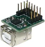
Figure 1 - The MM232R Mini Development Module.
MM232R Mini USB-Serial UART Development Module Datasheet Version 1.00
© Future Technology Devices International Ltd. 2005
�3. MM232R Pin Out and Signal Descriptions
3.1 MM232R Pin Out
MM232R 1 2
Page �
© FTDI 2005 3 5 7 10 12 16 15 14 4 6 8 9 11 13
Figure 2 - Module Pin Out.
SHIELD 1
VCC 2
VCCIO 3
VCC30 4
2.54mm (0.1")
TXD 5 RXD 7
RTS# 6 CTS# 8 13.30mm (0.52")
2.54mm (0.1")
SLEEP# 10
CLK12M 9
PWREN 12
RESET# 11
SHIELD 16
USBPWR 15
VCC50 14
GND 13
8.20mm (0.32")
Figure 3 - MM232R Signal pin out and PCB pad layout.
MM232R Mini USB-Serial UART Development Module Datasheet Version 1.00
© Future Technology Devices International Ltd. 2005
�3.2 Signal Descriptions
Table 1 - Module Pin Out Description Pin No. Name
1 2 SHEILD VCC
Page �
Type
GND PWR or Input
Description
USB Cable shield. To power the module from the 5V supply on USB bus connect pins 15 (USBPWR) and 14 (VCC50) together. In this case this pin becomes a 5V output, and can be used to supply the VCCIO pin, or to supply external logic. To use the MM232R module in a self powered configuration supply an external 3V - 5V supply to this pin, and do not connect together pins 15 and 14. +1.8V to +5.25V supply to the FT232RQ’s UART Interface and CBUS I/O pins. In USB bus powered designs connect to 3V3 to drive out at 3.3V levels (connect VCCIO to VCC3O), or connect to VCC to drive out at 5V CMOS level (connect VCCIO to VCC). This pin can also be supplied with an external 1.8V - 2.8V supply in order to drive out at lower levels. It should be noted that in this case this supply should originate from the same source as the supply to Vcc. This means that in bus powered designs a regulator which is supplied by the 5V on the USB bus should be used.
3
VCCIO
4
VCC3O
Output
3.3V output from integrated L.D.O. regulator. This pin is decoupled to ground on the module pcb with a 100nF capacitor. The prime purpose of this pin is to provide the internal 3.3V supply to the USB transceiver cell and the internal 1.5kΩ pull up resistor on USBDP. Up to 50mA can be drawn from this pin to power external logic if required. This pin can also be used to supply the FT232RQ’s VCCIO pin by connecting this pin to pin 3 (VCCIO). Transmit Asynchronous Data Output.* Request To Send Control Output / Handshake signal.* Receive Asynchronous Data Input.* Clear to Send Control input / Handshake signal.* Configurable CBUS I/O Pin. Function of this pin is configured in the device internal EEPROM. Factory default pin function for the MM232R module is 12MHz Clock output. See CBUS Signal Options, Table 2.* Configurable CBUS I/O Pin. Function of this pin is configured in the device internal EEPROM. Factory default pin function for the MM232R module is SLEEP# - Goes low during USB suspend mode. Typically used to power down an external TTL to RS232 level converter I.C. in USB to RS232 converter designs. This pin is the FT232R’s CBUS4 See CBUS Signal Options, Table 2.* Can be used by an external device to reset the FT232R. If not required can be left unconnected, or pulled up to VCCIO. Configurable CBUS I/O Pin. Function of this pin is configured in the device internal EEPROM. Factory default pin function for the MM232R module is PWREN# - Goes low after the device is configured by USB, then high during USB suspend. Can be used to control power to external logic P-Channel logic level MOSFET switch. Enable the interface pull-down option when using the PWREN# pin in this way. See CBUS Signal Options, Table 2.* Module ground supply pins Module 3.3V - 5.25V power supply input. To power the module from the 5V supply on USB bus connect pins 15 (USBPWR) and 14 (VCC50) together. 5V Power output USB port. For a low power USB bus powered design, up to 100mA can be sourced from the 5V supply on the USB bus. A maximum of 500mA can be sourced from the USB bus in a high power USB bus powered design. Connect to Pin 14 (VCC50) to power the MM232R module from the USB bus. USB Cable shield.
5 6 7 8 9 10
TXD RTS# RXD CTS# CLK12 SLEEP#
Output Output Input Input Output Output
11 12
RESET# PWREN#
Input Output
13 14 15
GND VCC5O USBPWR
GND PWR Output
16
SHEILD
GND
* When used in Input Mode, these pins are pulled to VCCIO via internal 200kΩ resistors. These pins can be programmed to gently pull low during USB suspend ( PWREN# = “1” ) by setting an option in the internal EEPROM.
MM232R Mini USB-Serial UART Development Module Datasheet Version 1.00
© Future Technology Devices International Ltd. 2005
�3.3 CBUS Signal Options
Page �
The following options can be configured on the CBUS I/O pins. These options are all configured in the internal EEPROM using the utility software MPROG, which can be downloaded from the FTDI website. The default configuration is described in Section 8. Table 2 - CBUS Signal Options CBUS Signal Option Available On CBUS Pin...
TXDEN TXLED# RXLED# TX&RXLED# PWREN# CBUS0, CBUS1, CBUS2, CBUS3, CBUS4 CBUS0, CBUS1, CBUS2, CBUS3, CBUS4 CBUS0, CBUS1, CBUS2, CBUS3, CBUS4 CBUS0, CBUS1, CBUS2, CBUS3, CBUS4 CBUS0, CBUS1, CBUS2, CBUS3, CBUS4
Description
Enable transmit data for RS485 Transmit data LED drive - pulses low when transmitting data via USB. See FT232R datasheet for more details. Receive data LED drive - pulses low when receiving data via USB. See FT232R datasheet for more details. LED drive - pulses low when transmitting or receiving data via USB. See FT232R datasheet for more details. Goes low after the device is configured by USB, then high during USB suspend. Can be used to control power to external logic PChannel logic level MOSFET switch. Enable the interface pull-down option when using the PWREN# pin in this way. Goes low during USB suspend mode. Typically used to power down an external TTL to RS232 level converter I.C. in USB to RS232 converter designs. 48MHz Clock output. 24MHz Clock output. 12MHz Clock output. 6MHz Clock output. CBUS bit bang mode option. Allows up to 4 of the CBUS pins to be used as general purpose I/O. Configured individually for CBUS0, CBUS1, CBUS2 and CBUS3 in the internal EEPROM. A separate application note will describe in more detail how to use CBUS bit bang mode. Synchronous and asynchronous bit bang mode WR# strobe Output Synchronous and asynchronous bit bang mode RD# strobe Output
SLEEP#
CBUS0, CBUS1, CBUS2, CBUS3, CBUS4
CLK48 CLK24 CLK12 CLK6 CBitBangI/O
CBUS0, CBUS1, CBUS2, CBUS3, CBUS4 CBUS0, CBUS1, CBUS2, CBUS3, CBUS4 CBUS0, CBUS1, CBUS2, CBUS3, CBUS4 CBUS0, CBUS1, CBUS2, CBUS3, CBUS4 CBUS0, CBUS1, CBUS2, CBUS3
BitBangWRn BitBangRDn
CBUS0, CBUS1, CBUS2, CBUS3 CBUS0, CBUS1, CBUS2, CBUS3
MM232R Mini USB-Serial UART Development Module Datasheet Version 1.00
© Future Technology Devices International Ltd. 2005
�4. Module Dimensions
Figure 4 - MM232R Module Dimensions
21.50mm (0.85") 3.00mm (0.12") 18.0mm (0.71")
Page �
12.00mm (0.47")
2.55mm (0.1") 12.00mm (0.47") 2.90mm (0.11") 2.54mm (0.1")
10.75mm (0.42") 1.60mm (0.06")
21.20mm (0.83")
8.20mm (0.32")
0.65mm (0.03")
2.50mm (0.10")
13.30mm (0.52") 1.90mm (0.07")
The FT232RQ is supplied in a RoHS compliant 5mm x 5mm QFN 32 package. The package is lead ( Pb ) free and uses a ‘green’ compound. The date code format is YYXX where XX = 2 digit week number, YY = 2 digit year number. The MM232R module uses exclusivly lead free components. Both the I.C. device and the module are fully compliant with European Union directive 2002/95/EC.
MM232R Mini USB-Serial UART Development Module Datasheet Version 1.00
© Future Technology Devices International Ltd. 2005
�5. Device Characteristics and Ratings
5.1 Absolute Maximum Ratings
Page 10
The absolute maximum ratings for the FT232R devices are as follows. These are in accordance with the Absolute Maximum Rating System (IEC 60134). Exceeding these may cause permanent damage to the device. Table 3 - Absolute Maximum Ratings Parameter
Storage Temperature Floor Life (Out of Bag) At Factory Ambient ( 30°C / 60% Relative Humidity) Ambient Temperature (Power Applied) Vcc Supply Voltage D.C. Input Voltage - USBDP and USBDM D.C. Input Voltage - High Impedance Bidirectionals D.C. Input Voltage - All other Inputs D.C. Output Current - Outputs DC Output Current - Low Impedance Bidirectionals Power Dissipation (Vcc = 5.25V)
Value
-65°C to 150°C 168 Hours (IPC/JEDEC J-STD-033A MSL Level 3 Compliant)* -40°C to 85°C -0.5 to +6.00 -0.5 to +3.8 -0.5 to +(Vcc +0.5) -0.5 to +(Vcc +0.5) 24 24 500
Unit
Degrees C Hours
Degrees C. V V V V mA mA mW
* If devices are stored out of the packaging beyond this time limit the devices should be baked before use. The devices should be ramped up to a temperature of 125°C and baked for up to 17 hours.
5.2 DC Characteristics
DC Characteristics ( Ambient Temperature = -40 to 85oC ) Table 4 - Operating Voltage and Current Parameter
Vcc1 Vcc2 Icc1 Icc2
Description
VCC Operating Supply Voltage VCCIO Operating Supply Voltage Operating Supply Current Operating Supply Current
Min
3.3 1.8 50
Typ
15 70
Max
5.25 5.25 100
Units
V V mA
Conditions
Normal Operation USB Suspend*
μA
Table 5 - UART and CBUS I/O Pin Characteristics (VCCIO = 5.0V, Standard Drive Level) Parameter
Voh Vol Vin VHys
Description
Output Voltage High Output Voltage Low Input Switching Threshold Input Switching Hysteresis
Min
3.2 0.3 1.3 50
Typ
4.1 0.4 1.6 55
Max
4.9 0.6 1.9 60
Units
V V V mV
Conditions
I source = 2mA I sink = 2mA ** **
Table 6 - UART and CBUS I/O Pin Characteristics (VCCIO = 3.3V, Standard Drive Level) Parameter
Voh Vol Vin VHys
Description
Output Voltage High Output Voltage Low Input Switching Threshold Input Switching Hysteresis
Min
2.2 0.3 1.0 20
Typ
2.7 0.4 1.2 25
Max
3.2 0.5 1.5 30
Units
V V V mV
Conditions
I source = 1mA I sink = 2mA ** **
MM232R Mini USB-Serial UART Development Module Datasheet Version 1.00
© Future Technology Devices International Ltd. 2005
�Page 11
Table 7 - UART and CBUS I/O Pin Characteristics (VCCIO = 2.8V, Standard Drive Level) Parameter
Voh Vol Vin VHys
Description
Output Voltage High Output Voltage Low Input Switching Threshold Input Switching Hysteresis
Min
2.1 0.3 1.0 20
Typ
2.6 0.4 1.2 25
Max
3.1 0.5 1.5 30
Units
V V V mV
Conditions
I source = 1mA I sink = 2mA ** **
Table 8 - UART and CBUS I/O Pin Characteristics (VCCIO = 5.0V, High Drive Level) Parameter
Voh Vol Vin VHys
Description
Output Voltage High Output Voltage Low Input Switching Threshold Input Switching Hysteresis
Min
3.2 0.3 1.3 50
Typ
4.1 0.4 1.6 55
Max
4.9 0.6 1.9 60
Units
V V V mV
Conditions
I source = 6mA I sink = 6mA ** **
Table 9 - UART and CBUS I/O Pin Characteristics (VCCIO = 3.3V, High Drive Level) Parameter
Voh Vol Vin VHys
Description
Output Voltage High Output Voltage Low Input Switching Threshold Input Switching Hysteresis
Min
2.2 0.3 1.0 20
Typ
2.8 0.4 1.2 25
Max
3.2 0.6 1.5 30
Units
V V V mV
Conditions
I source = 3mA I sink = 8mA ** **
Table 10 - UART and CBUS I/O Pin Characteristics (VCCIO = 2.8V, High Drive Level) Parameter
Voh Vol Vin VHys
Description
Output Voltage High Output Voltage Low Input Switching Threshold Input Switching Hysteresis
Min
2.1 0.3 1.0 20
Typ
2.8 0.4 1.2 25
Max
3.2 0.6 1.5 30
Units
V V V mV
Conditions
I source = 3mA I sink = 8mA ** **
**Inputs have an internal 200kΩ pull-up resistor to VCCIO. Table 11 - RESET# and TEST Pin Characteristics Parameter
Vin VHys
Description
Input Switching Threshold Input Switching Hysteresis
Min
1.3 50
Typ
1.6 55
Max
1.9 60
Units
V mV
Conditions
Table 12 - USB I/O Pin (USBDP, USBDM) Characteristics Parameter
UVoh UVol UVse UCom UVDif UDrvZ
Description
I/O Pins Static Output ( High) I/O Pins Static Output ( Low ) Single Ended Rx Threshold Differential Common Mode Differential Input Sensitivity Driver Output Impedance
Min
2.8 0 0.8 0.8 0.2 26
Typ
Max
3.6 0.3 2.0 2.5
Units
V V V V V
Conditions
RI = 1.5kΩ to 3V3Out ( D+ ) RI = 15kΩ to GND ( D- ) RI = 1.5kΩ to 3V3Out ( D+ ) RI = 15kΩ to GND ( D- )
29
44
Ohms
***
***Driver Output Impedance includes the internal USB series resistors on USBDP and USBDM pins.
MM232R Mini USB-Serial UART Development Module Datasheet Version 1.00
© Future Technology Devices International Ltd. 2005
�5.3 EEPROM Reliability Characteristics
The internal 1024 bit EEPROM has the following reliability characteristicsTable 13 - EEPROM Characteristics Parameter Description
Data Retention Read / Write Cycles
Page 1�
Value
15 100,000
Unit
Years Cycles
5.4 Internal Clock Characteristics
The internal Clock Oscillator has the following characteristics. Table 14 - Internal Clock Characteristics Parameter Min
Frequency of Operation Clock Period Duty Cycle 11.98 83.19 45
Value Typical
12.00 83.33 50
Unit Max
12.02 83.47 55 MHz ns %
MM232R Mini USB-Serial UART Development Module Datasheet Version 1.00
© Future Technology Devices International Ltd. 2005
�6. Module Configurations
6.1 Bus Powered Configuration
Page 1�
VCC
MM232R 1 2
VCCIO
© FTDI 2005 3 5 7 10 12 4 6 8 9 11 13
RTS# TXD CTS# RXD CLK12M PWREN#
VCC
RTS# TXD CTS# RXD CLK_IN I/O
MCU
GND
16
15
14
USBPWR
VCC50
Figure 5 - Bus Powered Configuration Figure 5 illustrates the MM232R in a typical USB bus powered design configuration. This is done by connecting pin 15 (USBPWR) to pin 14 (VCC50). Pin 3 (VCCIO), the supply to the FT232RQ’s UART and CBUS IO pins, is connected to pin 2 (VCC). Doing this will make the UART and CBUS IO pins drive out at 5V levels. A USB Bus Powered device gets its power from the USB bus. Basic rules for USB Bus power devices are as follows – i) ii) On plug-in to USB, the device must draw no more than 100mA. On USB Suspend the device must draw no more than 500μA.
iii) A Bus Powered High Power USB Device (one that draws more than 100mA) should use PWREN# to keep the current below 100mA on plug-in and 500μA on USB suspend. iv) A device that consumes more than 100mA can not be plugged into a USB Bus Powered Hub. v) No device can draw more that 500mA from the USB Bus. Figure 5 also illustrates interfacing the MM232R module to a microcontroller (MCU) UART interface. This example uses TXD and RXD for transmission and reception of data, and RTS# / CTS# hardware handshaking. Also in this example the 12MHz clock output on pin 9 is used to clock the MCU. If the MCU is handling power management functions, then this can be done by connecting PWREN# to an I/O pin on the MCU.
MM232R Mini USB-Serial UART Development Module Datasheet Version 1.00
© Future Technology Devices International Ltd. 2005
�6.2 Self Powered Configuration
Page 1�
VCC
MM232R 1 2
VCCIO
© FTDI 2005 3 5 7 10 12 4 6 8 9 11 13
RTS# TXD CTS# RXD CLK12M PWREN# RESET#
3.3V – 5V VCC
RTS# TXD CTS# RXD CLK_IN I/O
MCU
GND
16
15
14
VCC50 4k7 3.3V – 5V VCC
10k
Figure 6 - Self Powered Configuration Figure 6 illustrates the MM232R in a USB self powered configuration. In this case an external supply is connected to the VCC50 pin. In this example pin 3 (VCCIO), the supply to the FT232RQ’s UART and CBUS IO pins, is connected to pin 2 (VCC). Doing this will make the UART and CBUS IO pins drive out at the same voltage level as VCC50. The configuration shown in Figure 5 can have a 3.3V - 5V supply. A USB Self Powered device gets its power from its own power supply and does not draw current from the USB bus. The basic rules for USB Self powered devices are as follows – i) ii) A Self Powered device should not force current down the USB bus when the USB Host or Hub Controller is powered down. A Self Powered Device can use as much current as it likes during normal operation and USB suspend as it has its own power supply.
iii) A Self Powered Device can be used with any USB Host and both Bus and Self Powered USB Hubs In this case the power descriptor in the internal EEPROM should be programmed to a value of zero (self powered). In order to meet requirement (i) the USB Bus Power is used to control the RESET# input pin of the FT232R device. When the USB Host or Hub is powered up the internal 1.5kΩ resistor on USBDP is pulled up to 3.3V, thus identifying the device as a full speed device to USB. When the USB Host or Hub power is off, RESET# will go low and the device will be held in reset. As RESET# is low, the internal 1.5kΩ resistor will not be pulled up to 3.3V, so no current will be forced down USBDP via the 1.5kΩ pull-up resistor when the host or hub is powered down. To do this pin 14 (USB) is connected to PU2 and PU1 is connected to RST#. Failure to do this may cause some USB host or hub controllers to power up erratically. Note : When the FT232R is in reset, the UART interface pins all go tri-state. These pins have internal 200kΩ pull-up resistors to VCCIO, so they will gently pull high unless driven by some external logic.
MM232R Mini USB-Serial UART Development Module Datasheet Version 1.00 © Future Technology Devices International Ltd. 2005
�6.3 USB Bus Powered with Power Switching Configuration
P-Channel Power MOSFET
s d
Page 15
Switched 5V Power to External Logic 0.1uF
VCC
MM232R 1 2
VCCIO
© FTDI 2005 3 5 7 10 12 4 6 8 9 11 13 g
0.1uF
TXD RXD PWREN# 1k
Soft Start Circuit
16
15
14
USBPWR
VCC50
Figure 7 - Bus Powered with Power Switching Configuration USB Bus powered circuits need to be able to power down in USB suspend mode in order to meet the