Future Technology Devices International Ltd UM232H Single Channel USB Hi-Speed FT232H Development Module Datasheet
Document Reference No.: FT_000367 Version 1.2 Issue Date: 2011-04-18
Future Technology Devices International Ltd (FTDI) Unit 1, 2 Seaward Place, Centurion Business Park, Glasgow, G41 1HH, United Kingdom Tel: +44 (0) 141 429 2777, Fax: +44 (0) 141 429 2758 E-Mail (Support): support1@ftdichip.com Web: http://www.ftdichip.com
Use of FTDI devices in life support and/or safety applications is entirely at the user’s risk, and the user agrees to defend, indemnify and hold harmless FTDI from any and all damages, claims, suits or expense resulting from such use. Copyright © 2011 Future Technology Devices International Limited
�Document Reference No.: FT_000367 UM232H Single Channel USB Hi-Speed FT232H Development Module Datasheet Version 1.2 Clearance No.: FTDI# 198
1
Introduction
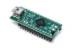
The UM232H is a USB-to-serial/FIFO development module in the FTDI product range which utilises the FT232H USB Hi-Speed (480Mb/s) single-port bridge chip to handle the USB signaling and protocols. The UM232H is ideal for development purposes to quickly prove functionality of adding USB to a target design. The UM232H is a module designed to plug into a standard 0.6” wide 28 pin DIP socket. The USB connection to a host system is via a mini-B USB connector. All components used, including the FT232H, are Pb-free (RoHS compliant).
Figure 1.1 : UM232H USB to Serial/FIFO Development Module
1.1 FT232H
The FT232H is a single channel USB 2.0 Hi-Speed (480Mb/s) to Serial/FIFO IC. It can be configured in a variety of serial or parallel interfaces, such as UART, FIFO or FTDI’s MPSSE mode which can configure either of the following interfaces: JTAG, SPI and I2C. For MPSSE mode, there is also 14 bit-banging lines available along with the four interface lines. In addition to these, the FT232H supports a CPU-Style FIFO mode and a fast serial interface mode. It also introduces a half-duplex FT1248 interface that provides a flexible data communication and high performance interface between the FT232H device and external logic. For further details on the FT232H and the FT1248 mode, please refer to the FT232H datasheet and application note: AN_167 FT1248 Parallel Serial Interface Basics, located at the FTDI website.
1 © Copyright 2011 Future Technology Devices International Ltd
�Document Reference No.: FT_000367 UM232H Single Channel USB Hi-Speed FT232H Development Module Datasheet Version 1.2 Clearance No.: FTDI# 198
Table of Contents 1 2 Introduction ....................................................................................... 1
1.1 2.1 2.2 2.3 FT232H ............................................................................................................... 1 Driver Support ................................................................................................. 3 Part Numbers ................................................................................................... 3 Features ............................................................................................................. 4 Key Features .................................................................................................... 5 UM232H Pin Out ............................................................................................. 7 Signal Descriptions ........................................................................................ 8 ACBUS Signal Options................................................................................. 11
Typical Applications ........................................................................ 3
3 4
FT232H Features and Enhancement.......................................... 5
3.1 4.1 4.2 4.3
UM232H Pin Out and Signal Descriptions................................ 7
5 6 7
Module Dimensions ....................................................................... 12 FT232H Device Characteristics and Ratings ......................... 13
6.1 7.1 7.2 7.3
7.3.1 7.3.2
DC Characteristics ........................................................................................ 13 BUS Powered Configuration ..................................................................... 14 USB Bus Powered with Power Switching Configuration ............................... 15 Self Powered Configuration ..................................................................... 16
Self-Powered Configuration with 3V3 I/O and running on +5V external supply: ..... 16 Self-Powered Configuration with 3V3 I/O and running on +3.3V external supply: .. 18
Module Configurations ................................................................. 14
8 9
UM232H Module Circuit Schematic .......................................... 19 EEPROM Configuration ................................................................. 20
Appendix A – List of Tables and Figures ........................................................ 23
10 Contact Information ...................................................................... 21 Appendix B – Revision History ........................................................ 24
2 © Copyright 2011 Future Technology Devices International Ltd
�Document Reference No.: FT_000367 UM232H Single Channel USB Hi-Speed FT232H Development Module Datasheet Version 1.2 Clearance No.: FTDI# 198
2
Typical Applications
Rapid USB integration into existing and new electronic systems USB to multi-port JTAG, SPI and I2C interfaces USB to FT1248 interfaces USB to RS232 / RS422 / RS485 Converters USB Instrumentation USB Industrial Control USB Electronic Point Of Sale Control Upgrading Legacy Peripherals to USB Cellular and Cordless Phone USB data transfer cables and interfaces Interfacing MCU / PLD / FPGA based designs to USB USB Audio and Low Bandwidth Video data transfer PDA to USB data transfer USB Smart Card Readers USB MP3 Player Interface USB FLASH Card Reader / Writers Set Top Box PC - USB interface USB Digital Camera Interface USB Hardware Modems USB Wireless Modems USB Bar Code Readers USB Software / Hardware Encryption Dongles USB Medical applications
The UM232H module can be used for prototyping and evaluation in an application using the FT232H.
2.1 Driver Support
The UM232H development module requires USB device drivers, available free from FTDI website. There is the Virtual Com Port driver which allows the UM232H to appear as a serial port allowing legacy applications for serial ports to function over USB (for example TTY). Another FTDI USB driver, the D2XX driver, can also be used with application software to directly access the FT232H on the UM232H through a DLL. Supported platforms include: current Microsoft® Windows® operating systems, Linux®, Mac OS® and Microsoft Windows CE® version 4.2 onwards.
2.2 Part Numbers
Part Number Description
UM232H
Development module for FT232H
3 © Copyright 2011 Future Technology Devices International Ltd
�Document Reference No.: FT_000367 UM232H Single Channel USB Hi-Speed FT232H Development Module Datasheet Version 1.2 Clearance No.: FTDI# 198
2.3 Features
The UM232H has the following features: Based on the Single chip USB Hi-Speed FT232H device. USB 2.0 Hi-Speed (480Mbits/Second) and Full Speed (12Mbits/Second) compatible Entire USB protocol handled on the chip – No USB-specific firmware programming required. Small USB Type B connector common on many commercial devices USB bus or self powered options. Asynchronous UART transfer data rate up to 12Mbaud. UART interface support for 7 or 8 data bits, 1 or 2 stop bits and odd / even / mark / space / no parity. Fully assisted hardware or X-On / X-Off software handshaking. Auto-transmit buffer control for RS485 applications. Supports a half duplex FT1248 interface with a bi-directional data bus (1, 2, 4 or 8 bits wide). Synchronous Serial (MPSSE) data rates of up to 30Mbps on JTAG, SPI and I2C Support for USB suspend and resume UHCI / OHCI / EHCI host controller compatible FTDI’s royalty-free VCP and D2XX drivers eliminate the requirement for USB driver development in most cases. 1kByte receive and transmit buffers for high data throughput. Transmit and receive LED drive signals. Adjustable receive buffer timeout. Synchronous and asynchronous bit bang mode interface options with RD# and WR# strobes. Support for USB suspend and resume. Integrated 3.3V level converter for USB I/O. USB bulk transfer mode. +2.97V to +5.25V Single Supply Operation. Low operating and USB suspend current. Low USB bandwidth consumption. -40°C to +85°C operating temperature range Reduce development time Rapid integration into existing systems
4 © Copyright 2011 Future Technology Devices International Ltd
�Document Reference No.: FT_000367 UM232H Single Channel USB Hi-Speed FT232H Development Module Datasheet Version 1.2 Clearance No.: FTDI# 198
3
FT232H Features and Enhancement 3.1 Key Features
USB Hi-Speed to UART/FIFO Interface. The FT232H provides a USB 2.0 Hi-Speed (480Mbits/s) to flexible and configurable UART/FIFO Interfaces. Functional Integration. The FT232H integrates a USB protocol engine, which controls the physical Universal Transceiver Macrocell Interface (UTMI) and handles all aspects of the USB 2.0 Hi -Speed interface. The FT232H includes an integrated +1.8V/3.3V Low Drop -Out (LDO) regulator. It also includes 1Kbytes Tx and Rx data buffers. The FT232H integrates the entire USB protocol on a chip with no firmware required. MPSSE. Multi-Protocol Synchronous Serial Engines (MPSSE), capable of speeds up to 30 Mbits/s, provides flexible synchronous interface configurations. FT1248 interface. The FT232H supports a half-duplex FT1248 interface with a bi-directional data bus interface that can be configured as 1, 2, 4 or 8-bits wide and this enables the flexibility to expand the size of the data bus to 8 pins. The FT1248 interface provides flexible data communication between an FT232H FT1248 slave and an external FT1248 master. The FT1248 interface consists of four signals called MIOSIO, the bi-directional data lines between the FT232H and an external master controller, SCLK which is the external clock input for latching data in or out the device at frequency up to 30MHz, SS_N Slave select input MISO which is the Master In Slave Out is an output from the FT232H in FT1248 mode. An external FT1248 master selects one of the FT1248 slave devices or enables the interface by pulling the Slave select input (SS_N) to logic 0. The FT1248 mode can be configured via the EEPROM settings with the free utility called FT_PROG which can be downloaded from the FTDI utilities page. For further details about FT1248 mode, see FT232H datasheet and application note AN_167 FT1248 Parallel Serial Interface Basics at the FTDI website. Data Transfer rate. The FT232H supports a data transfer rate up to 12 Mbaud when configured as an RS232/RS422/RS485 UART interface or up to 40 Mbytes/second over a synchronous 245 parallel FIFO interface or up to 8 Mbyte/Sec over an asynchronous 245 FIFO interface. Latency Timer. A feature of the driver used as a timeout to transmit short packets of data back to the PC. The default is 16ms, but it can be altered between 0ms and 255ms. Bus (ACBUS) functionality, signal inversion and drive strength selection. There are 11 configurable ACBUS I/O pins. These configurable options are: 1. 2. 3. 4. 5. 6. 7. 8. 9. 10. 11. TXDEN - transmit enable for RS485 designs. PWREN# - Power control for high power, bus powered designs. TXLED# - for pulsing an LED upon transmission of data. RXLED# - for pulsing an LED upon receiving data. TX&RXLED# - which will pulse an LED upon transmission OR reception of data. SLEEP# - indicates that the device going into USB suspend mode. CLK30 / CLK15 / CLK7.5 - 30MHz, 15MHz and 7.5MHz clock output signal options. TriSt-PU – Input pulled up, not used DRIVE 1 – Output driving high DRIVE 0 - Output driving low I/O mode – ACBUS Bit Bang
The ACBUS pins can also be individually configured as GPIO pins, similar to asynchronous bit bang mode. It is possible to use this mode while the UART interface is being used, thus providing up to 4 general purpos e I/O pins which are available during normal operation. The ACBUS lines can be configured with any one of these input/output options by setting bits in the external EEPROM Multi-Purpose UART/FIFO Controllers. The FT232H has one independent Serial/FIFO Controller. This controls the UART data, 245 FIFO data, Fast Serial (opto isolation) or Bit -Bang mode which can be selected by SETUP (SetBitMode) command. Each Multi-Purpose UART/FIFO Controller also contains an MPSSE
5 © Copyright 2011 Future Technology Devices International Ltd
�Document Reference No.: FT_000367 UM232H Single Channel USB Hi-Speed FT232H Development Module Datasheet Version 1.2 Clearance No.: FTDI# 198 (Multi-Protocol Synchronous Serial Engine). Using this MPSSE, the Multi-Purpose Serial/FIFO Controller can be configured under software command, to have one of the MPSSE interfaces (SPI, I2C, and JTAG). USB Protocol Engine and FIFO control. The USB Protocol Engine controls and manages the interface between the UTMI PHY and the FIFOs of the chip. It also handles power management and the USB protocol specification. Port FIFO TX Buffer (1Kbytes). Data from the Host PC is stored in these buffers to be used by the Multipurpose UART/FIFO controllers. This is controlled by the USB Protocol Engine and FIFO control block. Port FIFO RX Buffer (1Kbytes). Data from the Multi-purpose Serial/FIFO controllers is stored in these blocks to be sent back to the Host PC when requested. This is controlled by the USB Protocol Engine and FIFO control block.
RESET Generator – The integrated Reset Generator Cell provides a reliable power-on reset to the device internal circuitry at power up. The RESET# input pin allows an external device to reset the FT232H. RESET# should be tied to VCCIO (+3.3V) if not being used. Baud Rate Generators – The Baud Rate Generators provides a x16 or a x10 clock input to the UART’s from a 120MHz reference clock and consists of a 14 bit prescaler and 4 register bits which provide fine tuning of the baud rate (used to divide by a number plus a fraction). This determines the Baud Rate of the UART, which is programmable from 183 baud to 12 Mbaud. See FTDI application note AN_120 on the FTDI website for more details. EEPROM Interface. If the external EEPROM is fitted, the FT232H can be configured as an asynchronous serial UART (default mode), parallel FIFO (245) mode, FT1248, fast serial (opto isolation) or CPU-Style FIFO. The EEPROM should be a 16 bit wide configuration such as a 93LC56B or equivalent capable of a 1Mbit/s clock rate at VCCIO = +2.97V to 3.63V. The EEPROM is programmable in-circuit over USB using a utility program called FT_Prog available from FTDI web site. +1.8/3.3V LDO Regulator. The +3.3/+1.8V LDO regulator generates +1.8 volts for the core and the USB transceiver cell and +3.3V for the IO and the internal PLL and USB PHY power supply. UTMI PHY. The Universal Transceiver Macrocell Interface (UTMI) physical interface cell. This block handles the Full speed / Hi-Speed SERDES (serialise – deserialise) function for the USB TX/RX data. It also provides the clocks for the rest of the chip. A 12 MHz crystal must be connected to the OSCI and OSCO pins or 12 MHz Oscillator must be connected to the OSCI, and the OSCO is left unconnected. A 12K Ohm resistor should be connected between REF and GND on the PCB. The UTMI PHY functions include: Supports 480 Mbit/s “Hi-Speed” (HS)/ 12 Mbit/s “Full Speed” (FS). SYNC/EOP generation and checking Data and clock recovery from serial stream on the USB. Bit-stuffing/unstuffing; bit stuff error detection. Manages USB Resume, Wake Up and Suspend functions. Single parallel data clock output with on-chip PLL to generate higher speed serial data clocks.
6 © Copyright 2011 Future Technology Devices International Ltd
�Document Reference No.: FT_000367 UM232H Single Channel USB Hi-Speed FT232H Development Module Datasheet Version 1.2 Clearance No.: FTDI# 198
4
UM232H Pin Out and Signal Descriptions
4.1 UM232H Pin Out
The signal labels and pin designators for each are pin of the UM232H are illustrated in Fig. 4.1.
FTDI 2011
J2-1 – SLD VIO 3V3 PU2 PU1 GND AD0 AD1 AD2 AD3 AD4 AD5
GND
GND – J1-1 5V0 USB RST# AC9 AC8 AC7 AC6 AC5 AC4 AC3 AC2 AC1 AC0 – J1-14
AD6 J2-14 – AD7
Figure 4.1 : Module Pin Out
7 © Copyright 2011 Future Technology Devices International Ltd
�Document Reference No.: FT_000367 UM232H Single Channel USB Hi-Speed FT232H Development Module Datasheet Version 1.2 Clearance No.: FTDI# 198
4.2 Signal Descriptions
Pins marked * are EEPROM selectable
FT232H
Pin
ASYNC Serial (RS232) TXD RXD RTS# CTS# DTR# DSR# DCD# RI# SYNC 245 FIFO D0 D1 D2 D3 D4 D5 D6 D7 RXF# TXE# RD# WR SIWU# CLKOUT OE# PWRSAV#
Pin functions (depends on configuration)
STYLE ASYNC 245 FIFO D0 D1 D2 D3 D4 D5 D6 D7 RXF# TXE# RD# WR SIWU# ACBUS5 ACBUS6 PWRSAV# ASYNC Bit-bang D0 D1 D2 D3 D4 D5 D6 D7 ACBUS0 WRSTB# RDSTB# ACBUS3 SIWU# SYNC Bit-bang D0 D1 D2 D3 D4 D5 D6 D7 ACBUS0 WRSTB# RDSTB# ACBUS3 SIWU# Fast Serial interface FSDI FSCLK FSDO FSCTS ** TriSt-UP ** TriSt-UP ** TriSt-UP ** TriSt-UP CPU Style FIFO D0 D1 D2 D3 D4 D5 D6 D7 CS# A0 RD# WR SIWU#
Pin # Pin Name 13 ADBUS0 14 15 16 17 18 19 20 21 25 26 27 28 29 30 31 32 33 ADBUS1 ADBUS2 ADBUS3 ADBUS4 ADBUS5 ADBUS6 ADBUS7 ACBUS0 ACBUS1 ACBUS2 ACBUS3 ACBUS4 ACBUS5 ACBUS6 ACBUS7 ACBUS8 ACBUS9
MPSSE TCK/SK TDI/DO TDO/DI TMS/CS GPIOL0 GPIOL1 GPIOL2 GPIOL3 GPIOH0 GPIOH1 GPIOH2 GPIOH3 GPIOH4 GPIOH5 GPIOH6 *** GPIOH7
FT1248 MIOSI0 MIOSI1 MIOSI2 MIOSI3 MIOSI4 MIOSI5 MIOSI6 MIOSI7 SCLK SS_N MISO ACBUS3 ACBUS4 ACBUS5 ACBUS6 PWRSAV# ACBUS8 ACBUS9
*
TXDEN
**
ACBUS0
**
ACBUS1
**
ACBUS1
**
ACBUS2
**
ACBUS2
*
RXLED#
**
ACBUS3 SIWU#
*
TXLED#
**
ACBUS5
**
ACBUS5 ACBUS6 PWRSAV#
**
ACBUS5 ACBUS6 PWRSAV#
**
ACBUS5
**
ACBUS5
**
ACBUS6 PWRSAV#
**
ACBUS6 PWRSAV#
**
ACBUS6 PWRSAV# ** ACBUS8
**
ACBUS8
**
ACBUS8
**
ACBUS8
**
ACBUS8
**
ACBUS8
**
ACBUS8
**
ACBUS8
**
ACBUS9
**
ACBUS9
**
ACBUS9
**
ACBUS9
**
ACBUS9
**
ACBUS9
**
ACBUS9
**
ACBUS9
Table 4.1 : UM232H Signals
Pins marked ** default to tri-stated inputs with an internal 75KΩ (approx) pull up resistor to VCCIO. Pin marked *** default to GPIO line with an internal 75KΩ pull down resistor to GND. Using the EEPROM this pin can be enabled USBVCC mode instead of GPIO mode.
8 © Copyright 2011 Future Technology Devices International Ltd
�Document Reference No.: FT_000367 UM232H Single Channel USB Hi-Speed FT232H Development Module Datasheet Version 1.2 Clearance No.: FTDI# 198
The following 2 tables provide a description of the signals available on each pin of the UM232H module
Pin No. J1-1 J1-2 Name GND 5V0 Type PWR Input Description Module Ground Supply Pins +5.0V or +3.3V power supply input. 5V Power output USB port. For a low power USB bus powered design, up to 100mA can be sourced from the 5V supply on the USB bus. A maximum of 500mA can be sourced from the USB bus in a high power USB bus powered design. Can be used by an external device to reset the FT232H. If not required can be left unconnected, or pulled up to VCCIO Configurable ACBUS I/O Pin. Function of this pin is configured by EEPROM. The default configuration is TriSt-PU. See ACBUS Signal Options, Table 4.3 Configurable ACBUS I/O Pin. Function of this pin is configured by EEPROM. The default configuration is TriSt-PU. See ACBUS Signal Options, Table 4.3 Configurable ACBUS I/O Pin. Function of this pin is configured by EEPROM. The default configuration is TriSt-PD. See ACBUS Signal Options, Table 4.3 Configurable ACBUS I/O Pin. Function of this pin is configured by EEPROM. The default configuration is TriSt-PU. See ACBUS Signal Options, Table 4.3 Configurable ACBUS I/O Pin. Function of this pin is configured by EEPROM. The default configuration is TriSt-PU. See ACBUS Signal Options, Table 4.3 Configurable ACBUS I/O Pin. Function of this pin is configured by EEPROM. The default configuration is TriSt-PU. See ACBUS Signal Options, Table 4.3 Configurable ACBUS I/O Pin. Function of this pin is configured by EEPROM. The default configuration is TriSt-PU. See ACBUS Signal Options, Table 4.3 Configurable ACBUS I/O Pin. Function of this pin is configured by EEPROM. The default configuration is TriSt-PU. See ACBUS Signal Options, Table 4.3 Configurable ACBUS I/O Pin. Function of this pin is configured by EEPROM. The default configuration is TriSt-PU. See ACBUS Signal Options, Table 4.3 Configurable ACBUS I/O Pin. Function of this pin is configured by EEPROM. The default configuration is TriSt-PU. See ACBUS Signal Options, Table 4.3
J1-3
USB
Output
J1-4 J1-5 J1-6 J1-7 J1-8 J1-9 J1-10 J1-11 J1-12 J1-13 J1-14
RST# AC9 AC8 AC7 AC6 AC5 AC4 AC3 AC2 AC1 AC0
Input I/O I/O I/O I/O I/O I/O I/O I/O I/O I/O
Table 4.2 : UM232H Connector J1 Signal Description
9 © Copyright 2011 Future Technology Devices International Ltd
�Document Reference No.: FT_000367 UM232H Single Channel USB Hi-Speed FT232H Development Module Datasheet Version 1.2 Clearance No.: FTDI# 198
Pin No. J2-1 J2-2
Name SLD VIO
Type Shield to GND PWR
Description USB Cable Shield shorted to GND via a 0Ω resistor. 1.8 to +3.3V supply to the UART Interface and ACBUS I/O pins +3.3V output from the integrated L.D.O. regulator if the UM232H is running on 5V self or bus powered designs. Therefore this pin can be used to supply the FT232HL’s VCCIO pin by connecting this pin to J2-2 (VIO). This pin can also be an input if the UM232H is running on 3.3V self powered designs. Pull up resistor pin connection 1. Connect to J1-3 (USB) in a self powered configuration. Pull up resistor pin connection 2. Connect to J1-4 (RST#) in a self powered configuration. Module Ground Supply Pins Configurable Output Pin, the default configuration is Transmit Asynchronous Data Output / Handshake Signal.. Configurable Input Pin, the default configuration is Receiving Asynchronous Data Input / Handshake Signal.. Configurable Output Pin, the default configuration is Request to Send Control Output / Handshake Signal. Configurable Input Pin, the default configuration is Clear To Send Control Input / Handshake Signal. Configurable Output Pin, the default configuration is Data Terminal Ready Control Output / Handshake Signal. Configurable Input Pin, the default configuration is Data Set Ready Control Input / Handshake Signal. Configurable Input Pin, the default configuration is Data Carrier Detect Control Input / Handshake Signal.. Configurable Input Pin, the default configuration is RI#, Ring Indicator Control Input/ Handshake Signal. When remote wake up is enabled in the EEPROM taking RI# low >20ms can be used to resume the PC USB host controller from suspend.
J2-3
3V3
Output/Input
J2-4 J2-5 J2-6 J2-7 J2-8 J2-9 J2-10 J2-11 J2-12 J2-13
PU2 PU1 GND AD0 AD1 AD2 AD3 AD4 AD5 AD6
Control Control PWR Output Input Output Input Output Input Input
J2-14
AD7
Input
Table 4.3 : UM232H Connector J2 Signal Description Notes: 1. When used in Input Mode, the input pins are pulled to VCCIO via internal 75kΩ (approx.) resistors. These pins can be programmed to gently pull low during USB suspend (PWREN# = “1”) by setting an option in the EEPROM.
10 © Copyright 2011 Future Technology Devices International Ltd
�Document Reference No.: FT_000367 UM232H Single Channel USB Hi-Speed FT232H Development Module Datasheet Version 1.2 Clearance No.: FTDI# 198
4.3 ACBUS Signal Options
The table below describes the EEPROM options which can be configured on the ACBUS I/O pins using the software utility FT_PROG (which can be downloaded from the FTDI utilities page) The default EEPROM configuration is described in section 9.
ACBUS Signal Option
TXDEN
Available On ACBUS Pin
Description
ACBUS0, ACBUS1, ACBUS2, ACBUS3, ACBUS4, ACBUS5, ACBUS6, ACBUS8, ACBUS9 ACBUS0, ACBUS1, ACBUS2, ACBUS3, ACBUS4, ACBUS5, ACBUS6, ACBUS8, ACBUS9
TXDEN = (TTL level). Used with RS485 level converters to enable the line driver during data transmit. TXDEN is active from one-bit time before the start bit is transmitted on TXD until one bit time after the last stop bit. Output is low after the device has been configured by USB, then high during USB suspend mode. This output can be used to control power to external logic P-Channel logic level MOSFET switch. Enable the interface pull-down option when using the PWREN# in this way.* TXLED = Transmit signalling output. Pulses low when transmitting data (TXD) to the external device. This can be connected to an LED. RXLED = Receive signalling output. Pulses low when receiving data (RXD) from the external device. This can be connected to an LED. LED drive – pulses low when transmitting or receiving data from or to the external device. For more details, refer to the FT232H datasheet on the FTDI website. Goes low during USB suspend mode. Typically used to power down an external TTL to RS232 level converter IC in USB to RS232 converter designs. 30MHz Clock output. 15MHz Clock output. 7.5MHz Clock output. Input Pull Up
*PWREN#
TXLED#
ACBUS0, ACBUS1, ACBUS2, ACBUS3, ACBUS4, ACBUS5, ACBUS6, ACBUS8, ACBUS9 ACBUS0, ACBUS1, ACBUS2, ACBUS3, ACBUS4, ACBUS5, ACBUS6, ACBUS8, ACBUS9 ACBUS0, ACBUS1, ACBUS2, ACBUS3, ACBUS4, ACBUS5, ACBUS6, ACBUS8, ACBUS9 ACBUS0, ACBUS1, ACBUS2, ACBUS3, ACBUS4, ACBUS5, ACBUS6, ACBUS8, ACBUS9 ACBUS0, ACBUS5, ACBUS6,ACBUS8, ACBUS9 ACBUS0, ACBUS5, ACBUS6,ACBUS8, ACBUS9 ACBUS0, ACBUS5, ACBUS6,ACBUS8, ACBUS9 ACBUS0, ACBUS1, ACBUS2, ACBUS3, ACBUS4, ACBUS5, ACBUS6, ACBUS8, ACBUS9 ACBUS0, ACBUS5, ACBUS6,ACBUS8, ACBUS9 ACBUS0, ACBUS1, ACBUS2, ACBUS3, ACBUS4, ACBUS5, ACBUS6, ACBUS8, ACBUS9 ACBUS5, ACBUS6,ACBUS8, ACBUS9
RXLED#
TX&RXLED#
SLEEP#
**CLK30 **CLK15 **CLK7.5 TriSt-PU
DRIVE 1 DRIVE 0
Output High Output Low
I/O mode
ACBUS BitBang
Table 4.4 : ACBUS Signal Option * A 10kΩ resistor pull up is also recommended. **When in USB suspend mode, the output clocks are also suspended.
11 © Copyright 2011 Future Technology Devices International Ltd
�Document Reference No.: FT_000367 UM232H Single Channel USB Hi-Speed FT232H Development Module Datasheet Version 1.2 Clearance No.: FTDI# 198
5
Module Dimensions
2.54
18.25 13.0
GND
15.24
5.3
FTDI 2011
10.0 43.0 44.5
8.0
1.6 14.9 2.0
4.1 Diameter 5.8 5.0 12.50 14.80 0.50
Figure 5.1 : UM232H Module Dimensions All dimensions are in millimetres. The UM232H module uses exclusively lead free components, and are fully compliant with European Union directive 2002/95/EC.
12 © Copyright 2011 Future Technology Devices International Ltd
�Document Reference No.: FT_000367 UM232H Single Channel USB Hi-Speed FT232H Development Module Datasheet Version 1.2 Clearance No.: FTDI# 198
6
FT232H Device Characteristics and Ratings
6.1 DC Characteristics
The I/O signal levels are +3.3V, and all IO pins are +5V tolerant (except the USB PHY pins). DC Characteristics (Ambient Temperature = -40°C to +85°C)
Parameter VCCIO* VREGIN Ireg Icc5v0 Icc3v3 Description VCCIO Operating Supply Voltage VREGIN Voltage regulator Input Regulator Output Current UM232H current drawn UM232H current drawn 2 1.2 62 59 Minimum 2.97 3.6 5 Typical Maximum 3.63 5.5 100 Units V V mA mA mA Conditions Cells are 5V tolerant +5V Supply +3V3 Output +5V Supply +3.3V Supply
Table 6.1 : Operating Voltage and Current (except PHY) *NOTE: Failure to connect all VCCIO pins the device will have unpredictable behaviour. For the electrical characteristics of the FT232H device, please refer to the FT232H datasheet
13 © Copyright 2011 Future Technology Devices International Ltd
�Document Reference No.: FT_000367 UM232H Single Channel USB Hi-Speed FT232H Development Module Datasheet Version 1.2 Clearance No.: FTDI# 198
7
Module Configurations
The UM232H Module can be configured as USB Bus-Powered or USB Self-Powered. This section describes how to configure the UM232H for a number of different power supply arrangement s.
7.1 BUS Powered Configuration
Bus powered configuration, where the +5V supply that powers the module is sourced from the USB bus, and the 3V3 regulator output powers the core of the FT232H.
5V or 3V3
FTDI 2011
J2-1 VIO 3V3 5V0 USB
J1-1
MCU
RXD TXD CTS# RTS# TXD RXD RTS# CTS#
GND
J2-14
J1-14
Figure 7.1 : Bus Powered Configuration Figure 7.1 illustrates the UM232H in a typical USB bus powered design configuration , which consists of two connections, a J1-2 to J1-3 connection and a J2-2 to J2-3 connection. Connecting J1-2 (5V0) to J1-3 (USB) takes the power from the VBUS pin (J1-3) and supplies it to the on chip voltage regulator input of the FT232H via pin 5V0 (J1-2). Connecting J2-2 (VIO) (power input for core of the FT232H) and J2-3 (3V3) (power output from the FT232H) powers the VCCIO, VPLL and VPHY pins of the FT232H chip. A USB Bus Powered device gets its power from the USB bus. Basic rules for USB Bus power devi ces are as follows – i) On plug-in to USB, the device must draw no more than 100mA. ii) On USB Suspend the device must draw no more than 500μA. iii) A Bus Powered High Power USB Device (one that draws more than 100mA) should use PWREN# to keep the current below 100mA on plug-in and 500μA on USB suspend. iv) A device that consumes more than 100mA cannot be plugged into a USB Bus Powered Hub. v) No device can draw more that 500mA from the USB Bus. Interfacing the UM232H module to a microcontroller (MCU), or other logic for a bus powered design would be done in exactly the same way as for Self-Powered designs (see Section 7.3), except that the MCU or external logic would take its power supply from the USB bus (either the 5V on the USB pin, or 3.3V on the 3V3 pin).
14 © Copyright 2011 Future Technology Devices International Ltd
�Document Reference No.: FT_000367 UM232H Single Channel USB Hi-Speed FT232H Development Module Datasheet Version 1.2 Clearance No.: FTDI# 198
7.2
USB Bus Powered with Power Switching Configuration
P-Channel Power MOSFET s 100K g Soft Start Circuit d 0.1uF 0.1uF
FTDI 2011
1K
J2-1 VIO 3V3 5V0 USB
J1-1
PWREN#
MCU
RXD TXD CTS# RTS# TXD RXD RTS# CTS#
GND
J2-14
J1-14
Figure 7.2 : Bus Powered with Power Switching Configuration USB Bus Powered circuits need to be able to power down in USB suspend mode in order to meet the