UMFT201XB, UMFT220XB and UMFT230XB Datasheet
Version 1.3
Document Reference No.: FT_000506
Clearance No.: FTDI# 272
Future Technology
Devices International
Ltd
Datasheet
UMFT201XB,
UMFT220XB,
UMFT230XB Breakout
Modules
USB to I2C/UART/FT1248 breakout modules
1
Introduction
1.1 Features
UMFT201XB,
UMFT220XB,
and
UMFT230XB
breakout
modules
utilize
FTDI’s
FT201XQ,
FT220XQ, and FT230XQ chips, respectively, to
convert USB to serial or parallel interfaces. These
modules support the following popular interfaces:
-
UMFT201XB bridges from USB to I2C IC.
-
UMFT220XB bridges from USB to a user chosen,
parallel bit interface, FTDI’s FT1248/SPI. Note:
2 out of the 4 I/0 lines are available for this
module.
-
2
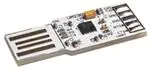
This module is a breakout board with a low profile. It
converts USB2.0 Full-Speed to a serial interface and
connects the serial signals to a 2.54mm (0.1”) pitch
10pin female receptacle. The boards do not use a USB
connector, but instead the modules plug directly into the
USB host connector and the pads of the PCB makes
electrical contact with the electrical contacts of the USB
connector.
All serial interfaces on these modules operate at +3.3V
voltage levels, however all I/Os are 5V tolerant.
UMFT230XB bridges from USB to UART IC.
Driver Support
Royalty-Free
DRIVERS for:
VIRTUAL
COM
PORT
(VCP)
Royalty-Free D2XX Direct Drivers (USB Drivers
+ DLL S/W Interface):
Windows 10 32,64-bit
Windows 10 32,64-bit
Windows 8 / 8.1 32,64-bit
Windows 8 / 8.1 32,64-bit
Windows 7 32,64-bit
Windows 7 32,64-bit
Windows Vista
Windows Vista
Windows XP 32,64-bit
Windows XP 32,64-bit
Windows XP Embedded
Windows XP Embedded
Windows CE.NET 4.2-5.2, 6.0/7.0, 2013
Windows CE.NET 4.2, 5.0 and 6.0
MAC OS-X
MAC OS OS-X
Linux 3.2 and greater
Linux 3.0 and greater
Android
Android
The drivers listed above are all available to download for free from www.ftdichip.com. Various 3rd Party
Drivers are also available for various other operating systems - visit www.ftdichip.com for details.
Copyright © Future Technology Devices International Limited
1
�UMFT201XB, UMFT220XB and UMFT230XB Datasheet
Version 1.3
Document Reference No.: FT_000506
3
Clearance No.: FTDI#
272
Ordering Information
Module
Interface
Features
UMFT201XB-01
I2C
USB to I2C with four control bus lines, 3.3V power out (with a 50mA
current limit) and fused 5V. Standard option, connector fitted to CN2.
UMFT201XB-NC
I2C
USB to I2C with four control bus lines, 3.3V power out (with a 50mA
current limit) and fused 5V. No connector option, no connector is fitted
to CN2.
UMFT201XB-WE
I2C
USB to I2C with four control bus lines, 3.3V power out (with a 50mA
current limit) and fused 5V. Wire ended option, 6” flying leads fitted to
CN2.
UMFT220XB-01
4-bit
FT1248
USB to FT1248 uses 2 FT1248 I/O lines, 3.3V power out (with a 50mA
current limit) and fused 5V. Standard option, connector fitted to CN2.
UMFT220XB-NC
4-bit
FT1248
USB to FT1248 uses 2 FT1248 I/O lines, 3.3V power out (with a 50mA
current limit) and fused 5V. No connector option, no connector is fitted
to CN2.
UMFT220XB-WE
4-bit
FT1248
USB to FT1248 uses 2 FT1248 I/O lines, 3.3V power out (with a 50mA
current limit) and fused 5V. Wire ended option, 6” flying leads fitted to
CN2.
UMFT230XB-01
Basic
UART
USB to UART with four control bus lines, 3.3V power out (with a 50mA
current limit) and fused 5V. UART rate can be up to 3 Mega Baud.
Standard option, connector fitted to CN2.
UMFT230XB-NC
Basic
UART
USB to UART with four control bus lines, 3.3V power out (with a 50mA
current limit) and fused 5V. UART rate can be up to 3 Mega Baud. No
connector option, no connector is fitted to CN2.
UMFT230XB-WE
Basic
UART
USB to UART with four control bus lines, 3.3V power out (with a 50mA
current limit) and fused 5V. UART rate can be up to 3 Mega Baud. Wire
ended option, 6” flying leads fitted to CN2.
Copyright © Future Technology Devices International Limited
2
�UMFT201XB, UMFT220XB and UMFT230XB Datasheet
Version 1.3
Document Reference No.: FT_000506
Clearance No.: FTDI#
272
Table of Contents
1
Introduction .................................................................... 1
1.1
Features .................................................................................... 1
2
Driver Support ................................................................ 1
3
Ordering Information ...................................................... 2
4
Signals and Configurations.............................................. 5
4.1
UMFT-XB Module Pin Outs ......................................................... 5
4.2
Signal Descriptions ................................................................... 5
4.3
UMFT201XB CN2 Signal Descriptions ........................................ 5
4.4
UMFT220XB CN2 Signal Descriptions ........................................ 6
4.5
UMFT230XB CN2 Signal Descriptions ........................................ 7
4.6
CBUS Signal Options ................................................................. 7
4.7
Configuring the MTP ROM ......................................................... 8
5
Module Dimensions ......................................................... 9
6
IC Package Markings ..................................................... 10
7
UMFT-XB-WE Module Wire Connections ........................ 11
8
9
7.1
UMFT201XB-WE Wire Connections .......................................... 11
7.2
UMFT220XB-WE Wire Connections .......................................... 12
7.3
UMFT230XB-WE Wire Connections .......................................... 12
Module Circuit Schematics ............................................ 13
8.1
UMFT201XB Schematic............................................................ 13
8.2
UMFT220XB Schematic............................................................ 13
8.3
UMFT230XB Schematic............................................................ 14
Environmental Compliances .......................................... 15
10 Internal MTP ROM Configuration ................................... 16
11 Contact Information ...................................................... 17
Appendix A - References .................................................... 15
Document References ..................................................................... 15
Acronyms and Abbreviations ........................................................... 15
Appendix B - List of Figures and Tables ............................. 16
List of Figures ................................................................................. 16
Copyright © Future Technology Devices International Limited
3
�UMFT201XB, UMFT220XB and UMFT230XB Datasheet
Version 1.3
Document Reference No.: FT_000506
Clearance No.: FTDI#
272
List of Tables ................................................................................... 16
Appendix C - Revision History ............................................ 17
Copyright © Future Technology Devices International Limited
4
�UMFT201XB, UMFT220XB and UMFT230XB Datasheet
Version 1.3
Document Reference No.: FT_000506
Clearance No.: FTDI#
272
Signals and Configurations
4
For all three modules, CN1 connects directly to a USB host or HUB port, or can be connected to a USB
extension cable. This connects the USB data signals, 5V USB Bus power and GND. When connecting these
modules to a USB host or HUB the USB signal pads should be facing upwards, and when connecting to
vertical connector the USB signal pad should be facing right. If the module is plugged in the wrong way,
no contact will be made between PCB and HUB, no damage will occur from plugging the module in upside
down.
4.1 UMFT-XB Module Pin Outs
Pin
UMFT201XB
UMFT220XB
UMFT230XB
1
SCL
IO0
TXD
2
VBUS
VBUS
VBUS
3
GND
GND
GND
4
RESET
RESET#
RESET#
5
SDA
SCK
RXD
6
3V3
3V3
3V3
7
CB0
SS#
RTS#
8
CB2
CB3
CB0
9
CB1
MISO
CTS#
10
CB3
IO1
Table 4.1 Module PinOut List
CB1
4.2 Signal Descriptions
Pin No.
Name
Type
Description
PWR
5V power input USB port. For a low power USB bus powered design, up to
100mA can be sourced from the 5V supply on the USB bus. A maximum of
500mA can be sourced from the USB bus in a high power USB bus powered
design.
1
VBUS
2
D-
Signal
Negative USB data signal
3
D+
Signal
Positive USB data signal
4
GND
PWR
Module Ground Supply
Table 4.2 CN1 PinOut Description
4.3 UMFT201XB CN2 Signal Descriptions
Pin No.
Name
Type
Description
1
SCL
Input
I2C clock input
2
VBUS
PWR
Outp
ut
5V Power output USB port.
3
GND
PWR
Module Ground Supply
4
RST#
Input
Can be used by an external device to reset the FT201X. If not required can be
left unconnected, or pulled up to VCCIO.
Copyright © Future Technology Devices International Limited
5
�UMFT201XB, UMFT220XB and UMFT230XB Datasheet
Version 1.3
Document Reference No.: FT_000506
Pin No.
Name
Type
5
SDA
I/O
6
3V3
Outp
ut
7
8
9
10
CB0
CB2
CB3
CB3
I/O
I/O
I/O
I/O
Clearance No.: FTDI#
272
Description
I2C bi-directional data line
3.3V output from integrated LDO regulator. This pin is decoupled to ground
on the module PCB with a 10nF capacitor. The prime purpose of this pin is to
provide the internal 3.3V supply to the USB transceiver cell.
Configurable CBUS I/O Pin. Function of this pin is configured in the device
internal
MTP ROM. Factory Default pin Function is PWREN#. See CBUS Signal Options,
Table 4.6
Configurable CBUS I/O Pin. Function of this pin is configured in the device
internal
MTP ROM. Factory Default pin Function is SLEEP#. See CBUS Signal Options,
Table 4.6
Configurable CBUS I/O Pin. Function of this pin is configured in the device
internal
MTP ROM. Factory Default pin Function is Tristate. See CBUS Signal Options,
Table 4.6
Configurable CBUS I/O Pin. Function of this pin is configured in the device
internal
MTP ROM. Factory Default pin Function is Tristate. See CBUS Signal Options,
Table 4.6
Table 4.3 I2C Module Pin Out Description
4.4 UMFT220XB CN2 Signal Descriptions
Pin No.
Name
Type
1
IO0
I/O
2
VBUS
PWR
Outp
ut
5V Power output USB port.
3
GND
PWR
Module Ground Supply
4
RST#
Input
Can be used by an external device to reset the FT220X. If not required can be
left unconnected, or pulled up to VCCIO.
5
SCK
Input
FT1248 Clock input from FT1248 interface master
6
3V3
Outp
ut
3.3V output from integrated LDO regulator. This pin is decoupled to ground
on the module PCB with a 10nF capacitor. The prime purpose of this pin is to
provide the internal 3.3V supply to the USB transceiver cell.
7
SS#
Input
FT1248 Chip select input to enable the device interface. Active low logic.
8
CB3
I/O
9
MISO
Outp
ut
10
IO1
I/O
Description
FT1248 Bi-Directional data bit 0
Configurable CBUS I/O Pin. Function of this pin is configured in the device
internal
MTP ROM. Factory Default pin Function is PWREN#. See CBUS Signal Options,
Table 4.6
Master In Serial Out. Used to provide status information to the FT1248
interface master.
FT1248 Bi-Directional data bit 1
Table 4.4 FT1248 Module Pin Out Description
Copyright © Future Technology Devices International Limited
6
�UMFT201XB, UMFT220XB and UMFT230XB Datasheet
Version 1.3
Document Reference No.: FT_000506
Clearance No.: FTDI#
272
4.5 UMFT230XB CN2 Signal Descriptions
Pin No.
Name
Type
Description
1
TXD
Outp
ut
UART Transmit Asynchronous Data Output.
2
VBUS
PWR
Outp
ut
5V Power output USB port.
3
GND
PWR
Module Ground Supply
4
RST#
Input
Can be used by an external device to reset the FT230X. If not required can be
left unconnected, or pulled up to VCCIO.
5
RXD
Input
UART Receiving Asynchronous Data Input.
6
3V3
Outp
ut
3.3V output from integrated LDO regulator. This pin is decoupled to ground
on the module PCB with a 10nF capacitor. The prime purpose of this pin is to
provide the internal 3.3V supply to the USB transceiver cell.
7
RTS#
Outp
ut
UART Request to Send Control Output / Handshake Signal.
8
CB0
I/O
9
CTS#
Input
10
CB1
I/O
Configurable CBUS I/O Pin. Function of this pin is configured in the device
internal
MTP ROM. Factory Default pin Function is PWREN#. See CBUS Signal Options,
Table 4.6
UART Clear To Send Control Input / Handshake Signal.
Configurable CBUS I/O Pin. Function of this pin is configured in the device
internal
MTP ROM. Factory Default pin Function is SLEEP#. See CBUS Signal Options,
Table 4.6
Table 4.5 UART Module Pin Out Description
4.6 CBUS Signal Options
CBUS Signal
Option
Available On CBUS Pin***
TRI-STATE
CBUS0, CBUS1, CBUS2,
CBUS3
IO Pad is tri-stated
DRIVE_1
CBUS0, CBUS1, CBUS2,
CBUS3
Output a constant 1
DRIVE_0
CBUS0, CBUS1, CBUS2,
CBUS3
Output a constant 0
TXDEN
CBUS0, CBUS1, CBUS2,
CBUS3
Enable transmit data for RS485 (Only in UMFT230XB)
PWREN#
CBUS0, CBUS1, CBUS2,
CBUS3
Output is low after the device has been configured by USB,
then high during USB suspend mode. This output can be
used to control power to external logic P-Channel logic level
MOSFET switch. Internal drive configuration consists of an
open drain to GND with no pull-up, specially designed for
battery charging applications.*
SLEEP#
CBUS0, CBUS1, CBUS2,
CBUS3
Goes low during USB suspend mode. Typically used to
power down an external TTL to RS232 level converter IC in
USB to RS232 converter designs.
Description
Copyright © Future Technology Devices International Limited
7
�UMFT201XB, UMFT220XB and UMFT230XB Datasheet
Version 1.3
Document Reference No.: FT_000506
Clearance No.: FTDI#
272
CBUS Signal
Option
Available On CBUS Pin***
CLK24MHz
CBUS0, CBUS1, CBUS2,
CBUS3
24 MHz Clock output.**
CLK12MHz
CBUS0, CBUS1, CBUS2,
CBUS3
12 MHz Clock output.**
CLK6MHz
CBUS0, CBUS1, CBUS2,
CBUS3
6 MHz Clock output.**
GPIO
CBUS0, CBUS1, CBUS2,
CBUS3
CBUS bit bang mode option. Allows up to 4 of the CBUS pins
to be used as general purpose I/O. Configured individually
for CBUS0, CBUS1, CBUS2 and CBUS3 in the internal MTP
ROM. A separate application note, AN232R-01, available
from FTDI website (www.ftdichip.com) describes in more
detail how to use CBUS bit bang mode.
BCD_Charger
CBUS0, CBUS1, CBUS2,
CBUS3
Battery charge Detect, indicates when the device is
connected to a dedicated battery charger host. Active high
output.
BCD_Charger#
CBUS0, CBUS1, CBUS2,
CBUS3
Inverse of BCD Charger
BitBang_WR#
CBUS0, CBUS1, CBUS2,
CBUS3
Synchronous and asynchronous bit bang mode WR# strobe
output.
BitBang_RD#
CBUS0, CBUS1, CBUS2,
CBUS3
Synchronous and asynchronous bit bang mode RD# strobe
output.
I2C_TXE#
CBUS0, CBUS1, CBUS2,
CBUS3
Transmit buffer empty, used to indicate to I2C master
device status of the FT201X transmit buffer
I2C_RXF#
CBUS0, CBUS1, CBUS2,
CBUS3
Receive buffer full, used to indicate to I2C master device
status of FT201X receive buffer
VBUS_Sense
CBUS0, CBUS1, CBUS2,
CBUS3
Input to detect when VBUS is present.
Time_Stamp
Description
CBUS0, CBUS1, CBUS2,
Toggle signal which changes state each time a USB SOF is
CBUS3
received
Table 4.6 CBUS Configuration Control
For further information on CBUS options, please refer to the relevant x-chip datasheet.
* PWREN# must be used with a 10kΩ resistor pull up.
**When in USB suspend mode the outputs clocks are also suspended.
***The number of CBUS pins available varies for the three different modules.
4.7 Configuring the MTP ROM
The IC on each of the modules contains an embedded MTP memory that can be used to specify the
functions of the CBUS pins, the current drive on each signal pin, current limit for the USB bus and the
descriptors of the device. For details on using the MTP ROM/EEPROM programming utility FT_PROG,
please see the FT_PROG User Guide.
When programming the MT memory please note:
i) The Max Bus Power setting of the MTP ROM should specify the maximum current to be drawn from
the USB host/hub when enumerated. For high-powered USB devices the current limit when
enumerated is between 100mA and 500mA, for low-powered USB devices the current limit is
100mA.
Copyright © Future Technology Devices International Limited
8
�UMFT201XB, UMFT220XB and UMFT230XB Datasheet
Version 1.3
Document Reference No.: FT_000506
5
Clearance No.: FTDI#
272
Module Dimensions
14.95
2.36
2.54
12.10
38.46
15.51
14.10
45.5
5.2
2.00
Measurements given in millimetres
Tolerance +/-0.1mm
Figure 5.1 UMFT-XB Module Dimensions
The UMFT201XB, UMFT220XB and UMFT230XB modules are mechanically identical. Figure 5.1 Uses
UMFT230 to illustrate the mechanical details.
Copyright © Future Technology Devices International Limited
9
�UMFT201XB, UMFT220XB and UMFT230XB Datasheet
Version 1.3
Document Reference No.: FT_000506
6
Clearance No.: FTDI#
272
IC Package Markings
1
FTDI
I
XXXXXXXXXX
12
FT201XQ
YYWW-D
5
8
The date code format is YYXX where XX = 2 digit week number, YY = 2 digit year number. This is
followed by the revision letter.
The code XXXXXXX is the manufacturing LOT code.
Copyright © Future Technology Devices International Limited
10
�UMFT201XB, UMFT220XB and UMFT230XB Datasheet
Version 1.3
Document Reference No.: FT_000506
7
Clearance No.: FTDI#
272
UMFT-XB-WE Module Wire Connections
7.1 UMFT201XB-WE Wire Connections
2
VBUS
2
SCL
1
1
ORANGE
SDA
5
5
YELLOW
CB0
7
7
GREEN
CB1
9
9
BROWN
CB2
8
8
GREY
CB3
10
10
RESET# 4
4
WHITE
6
BLUE
3
BLACK
3v3
GND
Wire 6"
6
3
RED
PURPLE
Figure 7.1 UMFT201XB-WE Wire Connections (numbers refer to pad numbers on the PCB)
Figure 6.1 illustrates the –WE product as a cable. This is only for illustration purposes. The wire ended
product consists of individual wires – not a cable
Copyright © Future Technology Devices International Limited
11
�UMFT201XB, UMFT220XB and UMFT230XB Datasheet
Version 1.3
Document Reference No.: FT_000506
Clearance No.: FTDI#
272
7.2 UMFT220XB-WE Wire Connections
2
2
VBUS
1
IO0
IO1
10
10
SCK
5
5
SS#
7
MISO
9
9
CB3
8
8
RESET# 4
4
3v3
ORANGE
YELLOW
GREEN
7
BROWN
Wire 6"
GREY
PURPLE
WHITE
6
6
GND
RED
1
BLUE
3
3
BLACK
Figure 7.2 UMFT220XB-WE Wire Connections (numbers refer to pad numbers on the PCB)
Figure 6.2 illustrates the –WE product as a cable. This is only for illustration purposes. The wire ended
product consists of individual wires – not a cable.
7.3 UMFT230XB-WE Wire Connections
VBUS
TXD
2
2
1
1
RXD
5
5
RTS#
7
7
CTS#
9
9
Wire 6"
CB0
8
8
CB1
10
10
4
4
RESET#
3v3
GND
6
3
6
3
RED
ORANGE
YELLOW
GREEN
BROWN
GREY
PURPLE
WHITE
BLUE
BLACK
Figure 7.3 UMFT230XB-WE Wire Connections (numbers refer to pad numbers on the PCB)
Figure 6.3 illustrates the –WE product as a cable. This is only for illustration purposes. The wire ended
product consists of individual wires – not a cable.
Copyright © Future Technology Devices International Limited
12
�UMFT201XB, UMFT220XB and UMFT230XB Datasheet
Version 1.3
Document Reference No.: FT_000506
8
Clearance No.: FTDI#
272
Module Circuit Schematics
8.1 UMFT201XB Schematic
Figure 8.1 UMFT201XB Circuit Schematic
8.2 UMFT220XB Schematic
Figure 8.2 UMFT220XB Circuit Schematic
Copyright © Future Technology Devices International Limited
13
�UMFT201XB, UMFT220XB and UMFT230XB Datasheet
Version 1.3
Document Reference No.: FT_000506
Clearance No.: FTDI#
272
8.3 UMFT230XB Schematic
Figure 8.3 UMFT230XB Circuit Schematic
Copyright © Future Technology Devices International Limited
14
�UMFT201XB, UMFT220XB and UMFT230XB Datasheet
Version 1.3
Document Reference No.: FT_000506
9
Clearance No.: FTDI#
272
Environmental Compliances
The UMFT-XB modules exclusively use lead free components, and are fully compliant with European
Union directive 2002/95/EC.
Copyright © Future Technology Devices International Limited
15
�UMFT201XB, UMFT220XB and UMFT230XB Datasheet
Version 1.3
Document Reference No.: FT_000506
Clearance No.: FTDI#
272
10 Internal MTP ROM Configuration
Following a power-on reset or a USB reset the FT-X chips will scan its internal MTP ROM and read the
USB configuration descriptors stored there. The default values programmed into the internal MTP ROM in
the FT201/220/230XB modules is shown in Table 10.1.
Parameter
Value
Notes
USB Vendor ID (VID)
0403h
FTDI default VID (hex)
USB Product UD (PID)
6015h
FTDI default PID (hex)
Serial Number Enabled?
Yes
Serial Number
See Note
A unique serial number is generated and
programmed into the MTP ROM during final test of
the FT201/220/230XB modules.
Pull down I/O Pins in USB
Suspend
Disabled
Enabling this option will make the device pull down
on the UART interface lines when the power is shut
off (PWREN# is high).
Manufacturer Name
FTDI
Product Description
UMFT201XB /
UMFT220XB /
UMFT230XB
Max Bus Power Current
Power Source
90mA
Bus Powered
Device Type
FT201X / FT220X /
FT230X
USB Version
0200
FT201X = 0x03, FT220X = 0x02, FT230X = 0x00
Returns USB 2.0 device description to the host.
Note: The device is a USB 2.0 Full Speed device
(12Mb/s).
Remote Wake Up
Enabled
Taking RI# low will wake up the USB host controller
from suspend.
High Current I/Os
Disabled
Enables the high drive level on the serial and CBUS
I/O pins.
Load VCP Driver
Enabled
Makes the device load the VCP driver interface for
the device.
UMFT201XB-01 CBUS0
GPIO
UMFT201XB-01 CBUS1
GPIO
UMFT201XB-01 CBUS2
GPIO
UMFT201XB-01 CBUS3
GPIO
UMFT220XB-01 CBUS3
Tristate
UMFT230XB-01 CBUS0
GPIO
UMFT230XB-01 CBUS1
GPIO
Table 10.1 Default Internal MTP ROM Configuration
The internal MTP ROM in the FT-X chip can be programmed over USB using the utility program FT_PROG.
FT_PROG can be downloaded from the www.ftdichip.com. Users who do not have their own USB vendor
ID but who would like to use a unique Product ID in their design can apply to FTDI for a free block of
unique PIDs. Contact FTDI Support (support1@ftdichip.com) for this service.
Copyright © Future Technology Devices International Limited
16
�UMFT201XB, UMFT220XB and UMFT230XB Datasheet
Version 1.3
Document Reference No.: FT_000506
Clearance No.: FTDI#
272
11 Contact Information
Head Office – Glasgow, UK
Branch Office – Hillsboro, Oregon, USA
Unit 1, 2 Seaward Place, Centurion Business Park
Glasgow G41 1HH
United Kingdom
Tel: +44 (0) 141 429 2777
Fax: +44 (0) 141 429 2758
7130 SW Fir Loop
Tigard, OR 97223
USA
Tel: +1 (503) 547 0988
Fax: +1 (503) 547 0987
E-mail (Sales)
E-mail (Support)
E-mail (General Enquiries)
E-Mail (Sales)
E-Mail (Support)
E-Mail (General Enquiries)
sales1@ftdichip.com
support1@ftdichip.com
admin1@ftdichip.com
us.sales@ftdichip.com
us.support@ftdichip.com
us.admin@ftdichip.com
Branch Office – Taipei, Taiwan
Branch Office – Shanghai, China
2F, No. 516, Sec. 1, NeiHu Road
Taipei 114
Taiwan, R.O.C.
Tel: +886 (0) 2 8797 1330
Fax: +886 (0) 2 8751 9737
Room 1103, No. 666 West Huaihai Road,
Shanghai, 200052
China
Tel: +86 (0)21 6235 1596
Fax: +86 (0)21 6235 1595
E-mail (Sales)
E-mail (Support)
E-mail (General Enquiries)
E-mail (Sales)
E-mail (Support)
E-mail (General Enquiries)
tw.sales1@ftdichip.com
tw.support1@ftdichip.com
tw.admin1@ftdichip.com
cn.sales@ftdichip.com
cn.support@ftdichip.com
cn.admin@ftdichip.com
Web Site
http://ftdichip.com
Distributor and Sales Representatives
Please visit the Sales Network page of the FTDI Web site for the contact details of our distributor(s) and sales
representative(s) in your country.
System and equipment manufacturers and designers are responsible to ensure that their systems, and any Future Technology Devices International Ltd
(FTDI) devices incorporated in their systems, meet all applicable safety, regulatory and system-level performance requirements. All application-related
information in this document (including application descriptions, suggested FTDI devices and other materials) is provided for reference only. While FTDI
has taken care to assure it is accurate, this information is subject to customer confirmation, and FTDI disclaims all liability for system designs and for any
applications assistance provided by FTDI. Use of FTDI devices in life support and/or safety applications is entirely at the user’s risk, and the user agrees to
defend, indemnify and hold harmless FTDI from any and all damages, claims, suits or expense resulting from such use. This document is subject to change
without notice. No freedom to use patents or other intellectual property rights is implied by the publication of this document. Neither the whole nor any part
of the information contained in, or the product described in this document, may be adapted or reproduced in any material or electronic form without the prior
written consent of the copyright holder. Future Technology Devices International Ltd, Unit 1, 2 Seaward Place, Centurion Business Park, Glasgow G41
1HH, United Kingdom. Scotland Registered Company Number: SC136640
Copyright © Future Technology Devices International Limited
17
�UMFT201XB, UMFT220XB and UMFT230XB Datasheet
Version 1.3
Document Reference No.: FT_000506
Clearance No.: FTDI#
272
Appendix A - References
Document References
AN232R-01
FT_PROG User Guide
Acronyms and Abbreviations
Terms
Description
DLL
Dynamic Link Library
BCD
Battery Charger Detection
EEPROM
Electrically Erasable Programmable Read Only Memory
I2C
Inter-Integrated Circuit
LDO
Low Drop Out Regulator
PCB
Printed Circuit Board
TTL
Transistor-Transistor Logic
USB
Universal Serial Bus
UART
VCP
Universal Asynchronous Receiver/Transmitter
Virtual COM Port
Copyright © Future Technology Devices International Limited
15
�UMFT201XB, UMFT220XB and UMFT230XB Datasheet
Version 1.3
Document Reference No.: FT_000506
Clearance No.: FTDI#
272
Appendix B - List of Figures and Tables
List of Figures
Figure 5.1 UMFT-XB Module Dimensions .......................................................................................... 9
Figure 7.1 UMFT201XB-WE Wire Connections (numbers refer to pad numbers on the PCB) .................. 11
Figure 7.2 UMFT220XB-WE Wire Connections (numbers refer to pad numbers on the PCB) .................. 12
Figure 7.3 UMFT230XB-WE Wire Connections (numbers refer to pad numbers on the PCB) .................. 12
Figure 8.1 UMFT201XB Circuit Schematic ....................................................................................... 13
Figure 8.2 UMFT220XB Circuit Schematic ....................................................................................... 13
Figure 8.3 UMFT230XB Circuit Schematic ....................................................................................... 14
List of Tables
Table 4.1 Module PinOut List .......................................................................................................... 5
Table 4.2 CN1 PinOut Description ................................................................................................... 5
Table 4.3 I2C Module Pin Out Description ......................................................................................... 6
Table 4.4 FT1248 Module Pin Out Description ................................................................................... 6
Table 4.5 UART Module Pin Out Description ...................................................................................... 7
Table 4.6 CBUS Configuration Control ............................................................................................. 8
Table 10.1 Default Internal MTP ROM Configuration ........................................................................ 16
Copyright © Future Technology Devices International Limited
16
�UMFT201XB, UMFT220XB and UMFT230XB Datasheet
Version 1.3
Document Reference No.: FT_000506
Clearance No.: FTDI#
272
Appendix C - Revision History
Document Title:
UMFT201XB, UMFT220XB, UMFT230XB Breakout Modules Datasheet
Document Reference No.:
FT_000506
Clearance No.:
FTDI# 272
Product Page:
http://www.ftdichip.com/FT-X.htm
Document Feedback:
Send Feedback
Revision
Changes
Date
Version 1.0
Initial Datasheet Created
2012-02-09
Version 1.1
Updated Photos and added Window
8 to driver support list
2013-01-31
Version 1.2
Updated -01 variant part number
2015-07-03
Version 1.3
Removed
TXLED/RXLED/TX&RXLED CBUS
functionality.
2019-02-21
Document template changes
made.
Copyright © Future Technology Devices International Limited
17
�