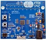
UMFT60x FIFO TO USB 3.0 Bridge Evaluation Board
Version 1.1
Document Reference No.:FT_001191
Clearance No.: FTDI#457
Future
Technology
Devices
International Ltd
UMFT60x
(FIFO TO USB 3.0
Bridge Evaluation
Board)
The UMFT60xx is an evaluation/development
module with either FMC(LPC)/HSMC connectors
for interfacing FTDI’s FT60x USB 3.0 Superspeed
IC with external hardware. The UMFT60xx allows
for bridging a FIFO bus to a USB3.0 host and
evaluating the functionality of the FT60x.
As a daughter card, the UMFT60xx must work
with a FIFO master board which has either a FMC
or HSMC connector. There are 4 models which
provide different FIFO bus interfaces and data bit
widths.
The modules are designed such that they can
plug into most FPGA development platforms
supplied by vendors such as Xilinx or Altera.
Refer to Ordering Information for module
options.
The UMFT60xx supports 2 parallel slave FIFO bus
protocols (Multi-Channel FIFO / 245 Synchronous
FIFO) with a data “burst” rate of up to 400MB/s.
For a full list of the FT60x’s features refer to the
FT60x datasheet.
The UMFT60xx module has the following features:
Supports USB 3.0 Super Speed (5Gbps)/USB
2.0 High Speed (480Mbps)/USB 2.0 Full Speed
(12Mbps) transfer
4 IN channels and 4 OUT channels on FIFO bus
connectivity
Supports multi voltage I/O: 1.8V, 2.5V and 3.3V
High speed connector for FIFO bus : FMC(Field
Programmable Mezzanine Card) or HSMC (High
Speed Mezzanine Card)
FMC connector is compatible with most Xilinx
FPGA reference design boards
HSMC is compatible with most Altera FPGA
reference design boards
Multi powered options: external DC powered,
BUS powered, FMC/HSMC powered
Hardware Reset and Remote Wake Up
Micro-USB3.0 receptacle
Neither the whole nor any part of the information contained in, or the product described in this manual, may be adapted or
reproduced in any material or electronic form without the prior written consent of the copyright holder. This product and its
documentation are supplied on an as-is basis and no warranty as to their suitability for any particular purpose is either made or
implied. Future Technology Devices International Ltd will not accept any claim for damages howsoever arising as a result of u se or
failure of this product. Your statutory rights are not affected. This product or any variant of it is not intended for use in any medical
appliance, device or system in which the failure of the product might reasonably be expected to result in personal injury. Th is
document provides preliminary information that may be subject to change without notice. No freedom to use patents or other
intellectual property rights is implied by the publication of this document. Future Technology Devices International Ltd, Unit 1, 2
Seaward Place, Centurion Business Park, Glasgow G41 1HH United Kingdom. Scotland Registered Company Number: SC136640
Copyright © Future Technology Devices International Limited
�UMFT60x FIFO TO USB 3.0 Bridge Evaluation Board
Version 1.1
Document Reference No.: FT_001191
Clearance No.: FTDI#457
1 Ordering Information
Part No.
Description
UMFT600A-B
16 Bit FIFO bus, HSMC connector with B version chip
UMFT601A-B
32 Bit FIFO bus, HSMC connector with B version chip
UMFT600X-B
16 Bit FIFO bus, FMC (Low Pin Count)connector with B version chip
UMFT601X-B
32 Bit FIFO bus, FMC(Low Pin Count) connector with B version chip
Table 1.1 UMFT60xx Ordering Information
Copyright © Future Technology Devices International Limited
1
�UMFT60x FIFO TO USB 3.0 Bridge Evaluation Board
Version 1.1
Document Reference No.: FT_001191
Clearance No.: FTDI#457
Table of Contents
1 Ordering Information ................................................ 1
2 Hardware Description ................................................ 3
2.1 Physical Description ............................................................5
2.1.1
Dimensions ........................................................................................ 5
2.2 Connectors, Jumpers and Push Buttons ..............................7
2.2.1
CN1 - Micro USB3.0 Receptacle ............................................................ 7
2.2.2
CN2 – POWER JACK 2.1MM .................................................................. 7
2.2.3
JP1 – External/VBUS Powered Selection ................................................. 7
2.2.4
JP2 – VCC33 Selection ......................................................................... 8
2.2.5
JP3, JP6– VCCIO Selection ................................................................... 8
2.2.6
JP4, JP5 –FIFO mode selection and GPIO pin out .................................... 8
2.2.7
SW1, SW2 – Push Buttons for Reset and Remote Wake Up ...................... 8
2.2.8
CN4 – FMC / HSMC FIFO bus interface connector .................................... 9
3 Board Schematics .................................................... 13
4 Hardware Setup Guide ............................................. 18
4.1 Power Configuration.......................................................... 18
4.2 Jumpers Default Position .................................................. 18
4.3 Power Consumption .......................................................... 19
5 Contact Information ................................................ 20
Appendix A – References ............................................. 21
Document References ............................................................... 21
Acronyms and Abbreviations..................................................... 21
Appendix B – List of Tables & Figures .......................... 22
List of Tables............................................................................. 22
List of Figures ........................................................................... 22
Appendix C – Revision History ..................................... 23
Copyright © Future Technology Devices International Limited
2
�UMFT60x FIFO TO USB 3.0 Bridge Evaluation Board
Version 1.1
Document Reference No.: FT_001191
Clearance No.: FTDI#457
2 Hardware Description
Figure 2-1 UMFT600A Module Top and Bottom View
Figure 2-2 UMFT601A Module Top and Bottom View
Figure 2-3 UMFT600X Module Top and Bottom View
Copyright © Future Technology Devices International Limited
3
�UMFT60x FIFO TO USB 3.0 Bridge Evaluation Board
Version 1.1
Document Reference No.: FT_001191
Clearance No.: FTDI#457
Figure 2-4 UMFT601X Module Top and Bottom View
The main functions of the UMFT60xx module are as follows:
Provides Multi-channel FIFO mode and 245 Synchronous FIFO mode Protocols, configured
by GPIOs.
Configurable FIFO clock: 66.67MHz and 100MHz (100MHz only for 2.5V or 3.3V VCCIO),
default clock is 100MHz.
High speed FIFO bus interface: FMC (Low Pin Count) and HSMC optional. See Ordering
Information.
Jumpers selection allowing powered options: VBUS-powered, External DC-powered, FIFO
master board-powered.
Multi voltage VCCIO option:1.8V, 2.5V, 3.3V.
Configurable GPIOs.
Hardware reset and remote wake up support.
Available with 16bit and 32bit wide FIFO bus.
Copyright © Future Technology Devices International Limited
4
�UMFT60x FIFO TO USB 3.0 Bridge Evaluation Board
Version 1.1
Document Reference No.: FT_001191
Clearance No.: FTDI#457
2.1 Physical Description
The UMFT600A/UMFT601A and UMFT600X/UMFT601X modules dimensions are illustrated in Figure
2.5 to Figure 2.8.
2.1.1 Dimensions
71.12
3.81
5.715
60.0
50.485
3.78
78.7
Figure 2-5 UMFT600A/UMFT601A Dimensions (Top view)
11.2
11.2
1.6
1.6
4.5
11.2
1.6
Figure 2-6 UMFT600A/UMFT601A Dimensions (Side view)
±0.10mm Tolerance
All dimensions are in mm
Copyright © Future Technology Devices International Limited
5
�UMFT60x FIFO TO USB 3.0 Bridge Evaluation Board
Version 1.1
Document Reference No.: FT_001191
Clearance No.: FTDI#457
63.56
3.515
11.33
60.0
70.0
Figure 2-7 UMFT600X/UMFT601X Dimensions (Top view)
11.2
1.6
6.3
Figure 2-8 UMFT600X/UMFT601X Dimensions (Side view)
±0.10mm Tolerance
All dimensions are in mm
Copyright © Future Technology Devices International Limited
6
�UMFT60x FIFO TO USB 3.0 Bridge Evaluation Board
Version 1.1
Document Reference No.: FT_001191
Clearance No.: FTDI#457
2.2 Connectors, Jumpers and Push Buttons
Connectors, jumpers and push buttons are described in the following sections.
2.2.1 CN1 - Micro USB3.0 Receptacle
Pin No.
Name
Type
Description
1
VBUS
P
5V DC power supply
2
D-
IO
USB D- line
3
D+
IO
USB D+ line
4
ID
IO
OTG identification(N.C.)
5
GND
P
Ground
6
SSTX-
O
Super Speed USB transmitter differential pair (-)
7
SSTX+
O
Super Speed USB transmitter differential pair(+)
8
GND
P
Ground
9
SSRX-
I
Super Speed USB receiver differential pair (-)
10
SSRX+
I
Super Speed USB receiver differential pair (+)
Table 2.1 CN1 - Micro USB3.0 Pin-out
2.2.2 CN2 – POWER JACK 2.1MM
Optional external DC 5V input.
Pin No.
Name
Type
Description
1
5V
P
5V power supply
2
GND
P
Ground
3
GND
P
Ground
Table 2.2 CN2 – POWER JACK 2.1MM
2.2.3 JP1 – External/VBUS Powered Selection
Select whether the module power is supplied by an external DC 5V or VBUS. Note this setting
must be chosen in conjunction with the JP2 setting. Default is open. [Note]
Jumper position
Description
Short pin 1-2
Select VBUS Power
Short pin 2-3
Select external DV 5V
Table 2.3 JP1 – 5V input Options
Copyright © Future Technology Devices International Limited
7
�UMFT60x FIFO TO USB 3.0 Bridge Evaluation Board
Version 1.1
Document Reference No.: FT_001191
Clearance No.: FTDI#457
2.2.4 JP2 – VCC33 Selection
Select whether the module main power is supplied by DC5V or the FIFO master board DC3.3V.[Note]
Jumper position
Description
Short pin 1-2
Select powered by external DV5V or VBUS
Short pin 2-3
Select powered by FIFO master Board(default)
Table 2.4 JP3 – VCC33 Option
2.2.5 JP3, JP6– VCCIO Selection
Select the IO voltage level.
[Note]
Jumper position
Description
JP3
JP6
Short pin 1-2
Open
VCCIO=2.5V(default)
Short pin 2-3
Open
VCCIO=1.8V
Open
Short
VCCIO=3.3V
Table 2.5 JP3 – VCCIO Option
2.2.6 JP4, JP5 –FIFO mode selection and GPIO pin out
Select Multi-channel FIFO mode or 245 Synchronous FIFO mode.
JP4 pin2 is GPIO_0 pin out and JP5 pin2 is GPIO_1 pin out.
Jumper position
GPIO valid
FIFO Mode
JP5
JP4
Channel
No.
GPIO_0
GPIO_1
(JP4 pin2)
(JP5 pin2)
1-2(or open)
1-2(or open)
Multi-Channel FIFO
4
Yes
Yes
1-2(or open)
2-3
Multi-Channel FIFO
2
Yes
No
2-3
1-2(or open)
Multi-Channel FIFO
1
No
Yes
2-3
2-3
245 Synchronous FIFO
1
No
No
Table 2.6 JP4, JP5 – Configurations
Note: Please refer to section 4 Hardware setup guide for more details power configuration options
and jumpers positions.
2.2.7 SW1, SW2 – Push Buttons for Reset and Remote Wake Up
SW1 – Reset, module hardware reset, mapped to FMC/HSMC connector, can be used for FIFO
master reset. Drive low when press down.
Copyright © Future Technology Devices International Limited
8
�UMFT60x FIFO TO USB 3.0 Bridge Evaluation Board
Version 1.1
Document Reference No.: FT_001191
Clearance No.: FTDI#457
SW2 – Remote Wake Up, drive low when press down.
2.2.8 CN4 – FMC / HSMC FIFO bus interface connector
2.2.8.1 FMC connector configurations-UMFT600X/UMFT601X Module
FMC Pin#/Name
UMFT600X
UMFT601X
U1: FT600 Pin#/Name
U1: FT601 Pin#/Name
C14/LA10_P
11 /Wake up_N (Optional, default: OPEN)
16 /Wake up_N (Optional, default: OPEN)
C15/LA10_N
10 /RESET_N
15 /RESET_N
C18/LA14_P
12 /GPIO_0(Optional, default: OPEN)
17 /GPIO_0(Optional, default: OPEN)
C19/LA14_N
13 /GPIO_1(Optional, default: OPEN)
18 /GPIO_1(Optional, default: OPEN)
C22/LA18_P_CC
43 /D_CLK (FIFO bus clock,FT600 output)
68 /D_CLK (FIFO bus clock,FT601 output)
C26/LA27_P
N.C.
62 /DATA18
C27_LA27_N
N.C.
60 /DATA16
D14/LA09_P
N.C.
8 /BE_N_3
D15/LA09_N
N.C.
7 /BE_N_2
D20/LA17_P_CC
N.C.
76 /DATA31
D21/LA17_N_CC
N.C.
75 /DATA30
D23/LA23_P
N.C.
70 /DATA25
D24/LA23_N
N.C.
69 /DATA24
D26/LA26_P
N.C.
63 /DATA19
D27/LA26_N
N.C.
61 /DATA17
G6/LA00_P_CC
N.C.
13 /OE_N
G7/LA00_N_CC
N.C.
12 /RD_N
G12/LA08_P
N.C.
11 /WR_N
G13/LA08_N
N.C.
10 /SIWU_N
G21/LA20_P
9 /OE_N
74 /DATA29
G22/LA20_N
8 /RD_N
73 /DATA28
G24/LA22_P
7 /WR_N
67 /DATA23
G25/_LA22_N
6 /SIWU_N
65 /DATA21
G27/LA25_P
56 /DATA15
57 /DATA15
G28/LA25_N
54 /DATA13
55 /DATA13
Copyright © Future Technology Devices International Limited
9
�UMFT60x FIFO TO USB 3.0 Bridge Evaluation Board
Version 1.1
Document Reference No.: FT_001191
FMC Pin#/Name
Clearance No.: FTDI#457
UMFT600X
UMFT601X
U1: FT600 Pin#/Name
U1: FT601 Pin#/Name
G30/LA29_P
48 /DATA11
53 /DATA11
G31/LA29_N
46 /DATA9
51 /DATA9
G33/LA31_P
42 /DATA7
47 /DATA7
G34/LA31_N
40 /DATA5
45 /DATA5
G36/LA33_P
36 /DATA3
43 /DATA3
G37/LA33_N
34 /DATA1
41 /DATA1
H13/LA07_P
N.C.
9 /RXF_N
H14/LA07_N
N.C.
8 /TXE_N
H19/LA15_P
N.C.
5 /BE_N_1
H20/LA15_N
N.C.
4 /BE_N_0
H22/LA19_P
5 /RXF_N
72 /DATA27
H23/LA19_N
4 /TXE_N
71 /DATA26
H25/LA21_P
3 /BE_N_1
66 /DATA22
H26/LA21_N
2 /BE_N_0
64 /DATA20
H28/LA24_P
55 /DATA14
56 /DATA14
H29/LA24_N
53 /DATA12
54 /DATA12
H31/LA28_P
47 /DATA10
52 /DATA10
H32/LA28_N
45 /DATA8
50 /DATA8
H34/LA30_P
41 /DATA6
46 /DATA6
H35/LA30_N
39 /DATA4
44 /DATA4
H37/LA32_P
35 /DATA2
42 /DATA2
H38/LA32_N
33 /DATA0
40 /DATA0
Table 2.7 CN4 – FMC connector configuration for FIFO bus
2.2.8.2 CN4 – HSMC connector configurations-UMFT600A/UMFT601A Module
HSMC
Pin#/Name
40 /CLKIN0
UMFT600A
UMFT601A
U1: FT600 Pin#/Name
U1: FT601 Pin#/Name
43 /D_CLK (FIFO bus clock,FT600 output)
68 /D_CLK (FIFO bus clock,FT601 output)
Copyright © Future Technology Devices International Limited
10
�UMFT60x FIFO TO USB 3.0 Bridge Evaluation Board
Version 1.1
Document Reference No.: FT_001191
HSMC
Pin#/Name
Clearance No.: FTDI#457
UMFT600A
UMFT601A
U1: FT600 Pin#/Name
U1: FT601 Pin#/Name
41 /D0
33 /DATA0
40 /DATA0
42 /D1
45 /DATA8
60 /DATA16
43 /D2
34 /DATA1
41 /DATA1
44 /D3
46 /DATA9
61 /DATA17
47 /D4
35 /DATA2
42 /DATA2
48 /D5
47 /DATA10
62 /DATA18
49 /D6
36 /DATA3
43 /DATA3
50 /D7
48 /DATA11
63 /DATA19
53 /D8
39 /DATA4
44 /DATA4
54 /D9
53 /DATA12
64 /DATA20
55 /D10
40 /DATA5
45 /DATA5
56 /D11
54 /DATA13
65 /DATA21
59 /D12
41 /DATA6
46 /DATA6
60 /D13
55 /DATA14
66 /DATA22
61 /D14
42 /DATA7
47 /DATA7
62 /D15
56 /DATA15
67 /DATA23
65 /D16
N.C.
50 /DATA8
66 /D17
2 /BE_N_0
69 /DATA24
67 /D18
N.C.
51 /DATA9
68 /D19
3 /BE_N_1
70 /DATA25
71 /D20
N.C.
52 /DATA10
72 /D21
4 /TXE_N
71 /DATA26
73 /D22
N.C.
53 /DATA11
74 /D23
5 /RXF_N
72 /DATA27
77 /D24
13 /GPIO_1(Optional, default: OPEN)
54 /DATA12
78 /D25
6 /SIWU_N
73 /DATA28
79 /D26
12 /GPIO_0(Optional, default: OPEN)
55 /DATA13
80 /D27
7 /WR_N
74 /DATA29
Copyright © Future Technology Devices International Limited
11
�UMFT60x FIFO TO USB 3.0 Bridge Evaluation Board
Version 1.1
Document Reference No.: FT_001191
HSMC
Pin#/Name
Clearance No.: FTDI#457
UMFT600A
UMFT601A
U1: FT600 Pin#/Name
U1: FT601 Pin#/Name
83 /D28
10 /RESET_N
56 /DATA14
84 /D29
8 /RD_N
75 /DATA30
85 /D30
11 /Wake up_N (Optional, default: OPEN)
57 /DATA15
86 /D31
9 /OE_N
76 /DATA31
101 /D40
N.C.
4 /BE_N_0
102 /D41
N.C.
8 /TXE_N
103 /D42
N.C.
5 /BE_N_1
104 /D43
N.C.
9 /RXF_N
107 /D44
N.C.
7 /BE_N_2
108 /D45
N.C.
10 /SIWU_N
109 /D46
N.C.
8 /BE_N_3
110 /D47
N.C.
11 /WR_N
113 /D48
N.C.
18 /GPIO_1(Optional, default: OPEN)
114 /D49
N.C.
12 /RD_N
115 /D50
N.C.
17 /GPIO_0(Optional, default: OPEN)
116 /D51
N.C.
13 /OE_N
119 /D52
N.C.
15 /RESET_N
121 /D54
N.C.
16 /Wake up_N (Optional, default: OPEN)
Table 2.8 CN4 – HSMC connector configuration for FIFO bus
Note: Refer to the FT600/FT601 device datasheet section 3 for details of the device pin out and
signal descriptions.
Copyright © Future Technology Devices International Limited
12
�UMFT60x FIFO TO USB 3.0 Bridge Evaluation Board
Version 1.1
Document Reference No.: FT_001191
Clearance No.: FTDI#457
3 Board Schematics
Figure 3-1 Schematics: Power for UMFT600A/UMFT600X/UMFT601A/UMFT601X
Copyright © Future Technology Devices International Limited
13
�UMFT60x FIFO TO USB 3.0 Bridge Evaluation Board
Version 1.1
Document Reference No.: FT_001191
Clearance No.: FTDI#457
Figure 3-2 Schematics: USB3.0 Bridge_UMFT600A/UMFT600X
Copyright © Future Technology Devices International Limited
14
�UMFT60x FIFO TO USB 3.0 Bridge Evaluation Board
Version 1.1
Document Reference No.: FT_001191
Clearance No.: FTDI#457
Figure 3-3 Schematics: USB3.0 Bridge_UMFT601A/UMFT601X
Copyright © Future Technology Devices International Limited
15
�UMFT60x FIFO TO USB 3.0 Bridge Evaluation Board
Version 1.1
Document Reference No.: FT_001191
Clearance No.: FTDI#457
Figure 3-4 Schematics: HSMC_UMFT600A
Figure 3-5 Schematics: HSMC_UMFT601A
Copyright © Future Technology Devices International Limited
16
�UMFT60x FIFO TO USB 3.0 Bridge Evaluation Board
Version 1.1
Document Reference No.: FT_001191
Clearance No.: FTDI#457
Figure 3-6 Schematics: FMC_UMFT600X
Figure 3-7 Schematics: FMC_UMFT601X
Copyright © Future Technology Devices International Limited
17
�UMFT60x FIFO TO USB 3.0 Bridge Evaluation Board
Version 1.1
Document Reference No.: FT_001191
Clearance No.: FTDI#457
4 Hardware Setup Guide
4.1 Power Configuration
There are 3 methods of powering the UMFT60xx module.
1) FIFO master board Power (3.3V)-Connect the UMFT60xx board to the FIFO master
board that has the standard configuration FMC (LPC or HPC) or HSMC female
connector. This method is the default setting and recommended.
2) USB Power (5V) - Connect USB power by micro-USB3.0 or micro-USB2.0 cable to CN1.
3) DC IN (5V) - Connect DC 5V to CN2.
The following table summarizes how to power the UMFT60xx module using the various methods.
Power Method
CN1
CN2
JP1
JP2
JP3 and JP6
FIFO master board
Power(Default and
Recommended)
-
N.C.
Open
Short pin 2-3
Follow FIFO master IO
voltage.
USB Power
5V
N.C.
Short pin1-2
Short pin1-2
DC IN(5V)
-
5V
Short pin2-3
Short pin1-2
Default:
JP3 short pin1-2
VCCIO=2.5V
JP6: Open
Table 4.1 Board Power Configuration
4.2 Jumpers Default Position
Jumper
JP1
JP2
JP3
JP4
JP5
JP6
Default Position
Open
2-3
1-2
1-2
1-2
Open
Table 4.2 Jumpers Default Position
Figure 4.1 shows the Jumpers’ locations on the PCB, and they are the same location on all 4
modules.
Figure 4-1 Jumpers Locations
Copyright © Future Technology Devices International Limited
18
�UMFT60x FIFO TO USB 3.0 Bridge Evaluation Board
Version 1.1
Document Reference No.: FT_001191
Clearance No.: FTDI#457
4.3 Power Consumption
Parameter
Description
Minimum
Typical
Maximum
IVCC_1
Units
Conditions
VCC Operating Supply Current
-
190
-
mA
Function Mode
IVCC_2
VCC Operating Supply Current
-
7.0
-
mA
Suspend Mode
IVBUS1
VBUS Operating Current
-
0.34
-
mA
DC/HSMC/FMC Powered,
Function and Suspend
Mode
IVBUS2
VBUS Operating Current
-
191
-
mA
VBUS-Powered Powered,
Function Mode
IVBUS3
VBUS Operating Current
-
7.3
-
mA
VBUS-Powered Powered,
Suspend Mode
Table 4.3 Power Consumption
Copyright © Future Technology Devices International Limited
19
�UMFT60x FIFO TO USB 3.0 Bridge Evaluation Board
Version 1.1
Document Reference No.: FT_001191
Clearance No.: FTDI#457
5 Contact Information
Head Office – Glasgow, UK
Branch Office – Tigard, Oregon, USA
Future Technology Devices International Limited
Unit 1, 2 Seaward Place, Centurion Business Park
Glasgow G41 1HH
United Kingdom
Tel: +44 (0) 141 429 2777
Fax: +44 (0) 141 429 2758
Future Technology Devices International Limited
(USA)
7130 SW Fir Loop
Tigard, OR 97223-8160
USA
Tel: +1 (503) 547 0988
Fax: +1 (503) 547 0987
E-mail (Sales)
E-mail (Support)
E-mail (General Enquiries)
sales1@ftdichip.com
support1@ftdichip.com
admin1@ftdichip.com
E-Mail (Sales)
E-Mail (Support)
E-Mail (General Enquiries)
us.sales@ftdichip.com
us.support@ftdichip.com
us.admin@ftdichip.com
Branch Office – Taipei, Taiwan
Branch Office – Shanghai, China
Future Technology Devices International Limited
(Taiwan)
2F, No. 516, Sec. 1, NeiHu Road
Taipei 114
Taiwan , R.O.C.
Tel: +886 (0) 2 8797 1330
Fax: +886 (0) 2 8751 9737
Future Technology Devices International Limited
(China)
Room 1103, No. 666 West Huaihai Road,
Shanghai, 200052
China
Tel: +86 21 62351596
Fax: +86 21 62351595
E-mail (Sales)
E-mail (Support)
E-mail (General Enquiries)
E-mail (Sales)
E-mail (Support)
E-mail (General Enquiries)
tw.sales1@ftdichip.com
tw.support1@ftdichip.com
tw.admin1@ftdichip.com
cn.sales@ftdichip.com
cn.support@ftdichip.com
cn.admin@ftdichip.com
Web Site
http://ftdichip.com
Distributor and Sales Representatives
Please visit the Sales Network page of the FTDI Web site for the contact details of our distributor(s) and sales
representative(s) in your country.
System and equipment manufacturers and designers are responsible to ensure that their systems, and any Future Technology
Devices International Ltd (FTDI) devices incorporated in their systems, meet all applicable safety, regulatory and system-level
performance requirements. All application-related information in this document (including application descriptions, suggested
FTDI devices and other materials) is provided for reference only. While FTDI has taken care to assure it is accurate, this
information is subject to customer confirmation, and FTDI disclaims all liability for system designs and for any applications
assistance provided by FTDI. Use of FTDI devices in life support and/or safety applications is entirely at the user’s risk, and the
user agrees to defend, indemnify and hold harmless FTDI from any and all damages, claims, suits or expense resulting from
such use. This document is subject to change without notice. No freedom to use patents or other intellectual property rights is
implied by the publication of this document. Neither the whole nor any part of the information contained in, or the product
described in this document, may be adapted or reproduced in any material or electronic form without the prior written consent
of the copyright holder. Future Technology Devices International Ltd, Unit 1, 2 Seaward Place, Centurion Business Park,
Glasgow G41 1HH, United Kingdom. Scotland Registered Company Number: SC136640
Copyright © Future Technology Devices International Limited
20
�UMFT60x FIFO TO USB 3.0 Bridge Evaluation Board
Version 1.1
Document Reference No.: FT_001191
Clearance No.: FTDI#457
Appendix A – References
Document References
FT600/FT601 datasheet: DS_FT600Q_FT601Q
D3xx Programmers Guide: AN379
Altera FPGA FIFO Master Programming Guide: AN377
Xilinx FPGA FIFO Master Programming Guide: AN376
Acronyms and Abbreviations
Terms
Description
FIFO
First In First Out
FMC
Field Programmable Mezzanine Card
HPC
High Pin Count
HSMC
IO
High Speed Mezzanine Card
Input Output
LPC
Low Pin Count
USB
Universal Serial Bus
Copyright © Future Technology Devices International Limited
21
�UMFT60x FIFO TO USB 3.0 Bridge Evaluation Board
Version 1.1
Document Reference No.: FT_001191
Clearance No.: FTDI#457
Appendix B – List of Tables & Figures
List of Tables
Table 1.1 UMFT60xx Ordering Information ............................................................................. 1
Table 2.1 CN1 - Micro USB3.0 Pin-out.................................................................................... 7
Table 2.2 CN2 – POWER JACK 2.1MM .................................................................................... 7
Table 2.3 JP1 – 5V input Options .......................................................................................... 7
Table 2.4 JP3 – VCC33 Option .............................................................................................. 8
Table 2.5 JP3 – VCCIO Option............................................................................................... 8
Table 2.6 JP4, JP5 – Configurations ....................................................................................... 8
Table 2.7 CN4 – FMC connector configuration for FIFO bus .................................................... 10
Table 2.8 CN4 – HSMC connector configuration for FIFO bus ................................................. 12
Table 4.1 Board Power Configuration ................................................................................... 18
Table 4.2 Jumpers Default Position ...................................................................................... 18
Table 4.3 Power Consumption ............................................................................................ 19
List of Figures
Figure 2-1 UMFT600A Module Top and Bottom View ............................................................... 3
Figure 2-2 UMFT601A Module Top and Bottom View ............................................................... 3
Figure 2-3 UMFT600X Module Top and Bottom View ............................................................... 3
Figure 2-4 UMFT601X Module Top and Bottom View ............................................................... 4
Figure 2-5 UMFT600A/UMFT601A Dimensions (Top view) ........................................................ 5
Figure 2-6 UMFT600A/UMFT601A Dimensions (Side view) ....................................................... 5
Figure 2-7 UMFT600X/UMFT601X Dimensions (Top view) ........................................................ 6
Figure 2-8 UMFT600X/UMFT601X Dimensions (Side view) ....................................................... 6
Figure 3-1 Schematics: Power for UMFT600A/UMFT600X/UMFT601A/UMFT601X ....................... 13
Figure 3-2 Schematics: USB3.0 Bridge_UMFT600A/UMFT600X ................................................ 14
Figure 3-3 Schematics: USB3.0 Bridge_UMFT601A/UMFT601X ................................................ 15
Figure 3-4 Schematics: HSMC_UMFT600A ............................................................................ 16
Figure 3-5 Schematics: HSMC_UMFT601A ............................................................................ 16
Figure 3-6 Schematics: FMC_UMFT600X .............................................................................. 17
Figure 3-7 Schematics: FMC_UMFT601X .............................................................................. 17
Figure 4-1 Jumpers Locations ............................................................................................. 18
Copyright © Future Technology Devices International Limited
22
�UMFT60x FIFO TO USB 3.0 Bridge Evaluation Board
Version 1.1
Document Reference No.: FT_001191
Clearance No.: FTDI#457
Appendix C – Revision History
Document Title:
UMFT60x FIFO TO USB 3.0 Bridge Evaluation Board
Document Reference No.:
FT_001191
Clearance No.:
FTDI#457
Product Page:
http://www.ftdichip.com/Products/ICs/FT600.html
Document Feedback:
Send Feedback
Revision
Changes
Date
1.0
Initial Release
2015-08-25
1.1
Updated ordering information to rev B
2016-10-17
Copyright © Future Technology Devices International Limited
23
�