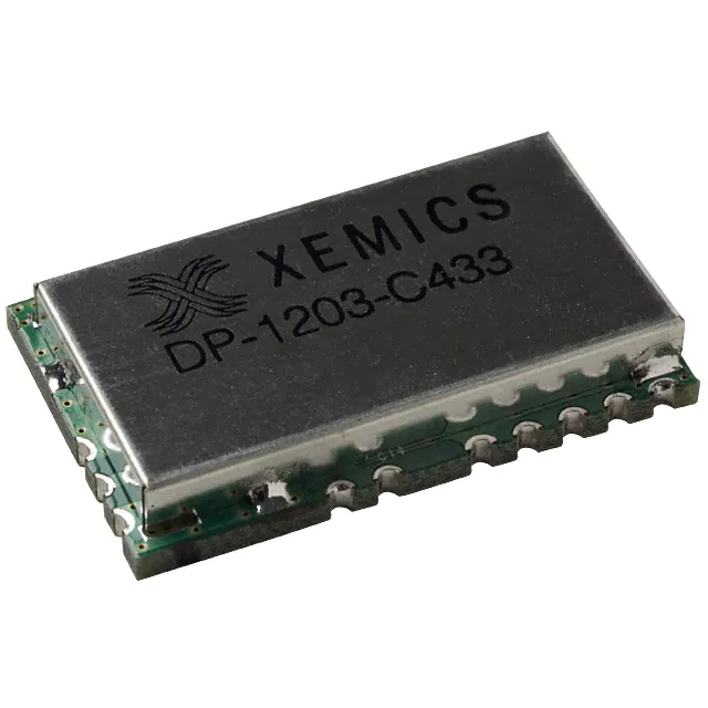
DP1203F
433/868/915 MHz RF Modules
DP1203F – C433 / 868 / 915
433, 868 and 915 MHz Drop-In RF Transceiver Modules
Combine Small Form Factor with High Performance
KEY PRODUCT FEATURES
GENERAL DESCRIPTION
•
•
•
•
•
•
The DP1203Fs are complete Radio Transceiver
Modules operating in the 433, 868 and 915 MHz
license free ISM (Industrial Scientific and Medical)
frequency bands. Based on the XE1203F
transceiver, the DP1203F offers the unique
advantage of high data rate communication up to
152.3 kbit/s. Combining high output power and
exceptional receiver sensitivity, the radio modules is
suitable for applications seeking to satisfy the
European (ETSI EN300-220-1 and EN301 439-3) or
the North American (FCC part 15.247 and 15.249)
regulatory standards.
•
•
•
•
•
•
•
•
•
The DP1203F modules can be used in any
environment where wireless remote connection is an
advantage. The DP1203F modules are perfect for
complex wireless networks involving high speed data
rate applications.
DEVICE OPTIONS
Part Number
APPLICATIONS
•
Home automation and access control
•
Wireless Network
•
Process and building control
No RF knowledge required
Direct Digital interface
Fully assembled and tested
Surface mount
30.5 mm x 18.5 mm
Available on tape&reel for Automatic assembly
system
Supply voltage 2.4 V – 3.6 V
Frequency synthesizer steps 500 Hz
Output power is programmable up to 15 dBm
High Rx 0.1% sensitivity down to -111 dBm
Data rate up to 152.3 kbit/s
Current consumption Tx=62 mA at15 dBm
Current consumption Rx=14 mA
Digital RSSI (Received Signal Strength Indicator)
Digital FEI (Frequency Error Indicator)
DP1203C4333LF
DP1203C8683LF
DP1203C9153LF
Rev 3 May 2006
Frequency band
433-435 MHz
868-870 MHz
902-928 MHz
Package
Board
Board
Board
www.semtech.com
1
�DP1203F
433/868/915 MHz RF Modules
Table of Contents
1
2
2.1
2.2
3
4
5
5.1
6
7
8
9
Pin Description ............................................................................................................................................3
Electrical Characteristics ...........................................................................................................................4
Absolute maximum operating ranges............................................................................................................4
Specifications ................................................................................................................................................5
Functional Description ...............................................................................................................................6
Serial Control Interface...............................................................................................................................7
Operation Modes .........................................................................................................................................8
Standard sequence for switching between receiver and transmitter ............................................................9
Typical Application ...................................................................................................................................10
Mechanical Dimensions............................................................................................................................11
Packaging Information..............................................................................................................................12
References .................................................................................................................................................12
© Semtech 2006
www.semtech.com
2
�DP1203F
433/868/915 MHz RF Modules
1
PIN DESCRIPTION
Pad Dimension
21
20
19
18
17
16
15
14
13
12
11
1.0
1.8
18.50
XE1203F
1
2
3
4
6
5
7
8
9
10
30.5
PIN
1
2
3
4
5
6
7
8
9
10
11
12
13
14
15
16
17
18
19
20
21
NAME
GND
RFIN/OUT
GND
VDDP
VDDA
GND
VDD
EN
SWITCH
GND
GND
SO
SI
SCK
CLKOUT
DCLK
DATA
DATAIN
PATTERN
RX
TX
I/O
IN
IN/OUT
IN
IN/OUT
OUT
IN
IN
OUT
OUT
IN/OUT
IN
OUT
IN
IN
DESCRIPTION
Ground
RF input / output terminal
Ground
Supply voltage / Advised NC
Supply voltage
Ground
Supply voltage
3-wire interface communication enable signal
Operating mode selection
Ground
Ground
Data output of the 3-wires interface
Data input of the 3-wires interface
Input clock of the 3-wires interface
Output clock at quartz frequency divided by 4, 8, 16 or 32
Transmitter or Receiver clock
Transmitter input data or Receiver output data
Transmitter input data
Output of the pattern recognition block
Antenna switch RX Select
Antenna switch TX select
© Semtech 2006
www.semtech.com
3
�DP1203F
433/868/915 MHz RF Modules
2
ELECTRICAL CHARACTERISTICS
2.1
ABSOLUTE MAXIMUM OPERATING RANGES
Description
Supply voltage
Operating temperature
Storage temperature
Soldering temperature (max 15 sec)
Min
2.4
-40
-55
Max
3.6
+85
125
260
Unit
V
o
C
o
C
o
C
CAUTION: ESD sensitive device.
Precaution should be taken when handling the device in order to prevent permanent damage
Life Support Policy and Use in Safety Critical Applications
SEMTECH PRODUCTS ARE NOT DESIGNED, INTENDED, AUTHORIZED OR WARRANTED TO BE SUITABLE
FOR USE IN LIFE-SUPPORT APPLICATIONS, DEVICES OR SYSTEMS OR OTHER CRITICAL APPLICATIONS.
INCLUSION OF SEMTECH PRODUCTS IN SUCH APPLICATIONS IS UNDERSTOOD TO BE UNDERTAKEN
SOLELY AT THE CUSTOMER’S OWN RISK.
© Semtech 2006
www.semtech.com
4
�DP1203F
433/868/915 MHz RF Modules
2.2 SPECIFICATIONS
The table below gives the specifications of the DP1203F under the following conditions:
Supply Voltage VDD = 3.3V, temperature = 25°C, 2-level FSK without pre-filtering, carrier frequency fc = 434 MHz
for DP1203C4333LF, fc = 869 MHz for DP1203C8683LF and fc = 915 MHz for DP1203C9153LF, frequency
deviation ∆f = 55 kHz, bit rate BR = 4.8kbps, Base band filter bandwidth BBW = 200 KHz, bit error rate BER = 0.1
% (measured at the output of the bit synchronizer), antenna output matched at 50 Ω.
Symbol
FR
Parameter
Synthesizer Frequency Range
Conditions
DP1203C4333LF
DP1203C8683LF
DP1203C9153LF
IDDSL
IDDST
IDDR
IDDT
Sleep mode supply current
Standby mode supply current
RX mode supply current
TX mode supply current
RFS
RF Sensitivity
A-mode, BR = 4.8 kbps /
BER = 0.1%
FDA
BR
Frequency Deviation
Bit rate
Programmable
Programmable
PRF
RF output power
Programmable.
RFOP1
RFOP2
RFOP3
RFOP4
TS_TR
TS_RE
TS_OS
Transmitter wake-up time
Receiver base-band wake up time
Quartz oscillator wake up time
XTAL
Quartz oscillator frequency
VIH
VIL
Digital input level high
Digital input level low
Min
433
868
902
Typ
-
Max
435
870
928
Units
MHz
MHz
MHz
0.2
0.85
14
33
62
1
1.1
17
40
75
uA
mA
mA
mA
mA
-111
-108
dBm
1
1.2
-
255
152.3
kHz
Kb/s
-3
+2
+7
+12
0
+5
+10
+15
-
dBm
dBm
dBm
dBm
-
150
0.5
1
250
0.8
2
39 MHz running
PRF = 5 dBm
PRF = 15dBm
From oscillator enabled
From oscillator enabled
Fundamental
39
% VDD
% VDD
75
-
© Semtech 2006
-
us
ms
ms
MHz
25
%
%
www.semtech.com
5
�DP1203F
433/868/915 MHz RF Modules
3
FUNCTIONAL DESCRIPTION
The True RF DP1203F is a cost effective high performance radio transceiver module designed for the wireless
transmission of digital information over distances of >500 meters in free space.
The module is based on the RF transceiver circuit from SEMTECH, the XE1203F. For more information on the
XE1203F, please refer to the XE1203F datasheet.
The module incorporates an antenna switch and a SAW Filter placed on the Rx path.
TX
RX
PATTERN DATAIN
SAW
DATA
DCLK CLKOUT
SCK
SI
SO
GND
LNA match
Xtal
39 MHz
XE1203F
PA match
RF
Switch
VCO
tank
Loop
filter
GND
RF IN/
OUT
GND
VDDP
VDDA
© Semtech 2006
GND
VDD
EN
SWITCH
GND
www.semtech.com
6
�DP1203F
433/868/915 MHz RF Modules
4
SERIAL CONTROL INTERFACE
A 3-wire bi-directional bus (SCK, SI, SO) is used to control the DP1203F. The output signal, SO, is provided by the
DP1203F in opposition to the SCK and SI which needs to be provided by the external application as an 8-bit
microcontroller. An access Read or Write with the XE1203F is possible only when the enable signal is active
(active LOW).
For more information about the 3-wire bus, please refer to the XE1203F datasheet chapter; Serial interface
definition and principles of operation.
sck
A(4)
si
A(3)
A(2)
A(1)
A(0) D(7) D(6) D(5)
D(4) D(3)
D(2) D(1) D(0)
/en
so
High impedance
Write sequence into configuration register
sck
A(4)
si
A(3)
A(2) A(1)
A(0)
/en
so
High impedance
D(7) D(6) D(5)
D(4) D(3)
D(2) D(1)
D(0) High impedance
Read sequence of configuration register
© Semtech 2006
www.semtech.com
7
�DP1203F
433/868/915 MHz RF Modules
5
OPERATION MODES
When operating the XE1203F, it might by useful to quickly switch between two pre-defined operating modes, to
save time and traffic on the 3-wire serial interface bus. This may occur when the XE1203F is required to switch
quickly between receive and transmit mode, when it has to operate on two different carrier frequencies, or when it
has to switch between the high linearity mode B and the high sensitivity mode A. For that purpose, the five
parameters stored in the SWParam Configuration Register are duplicated: the configuration set#1 and the
configuration set #2.
Depending on the ConfigSwitch 1-bit Register or the input level at the SWITCH pin, the XE1203F transceiver will
use either the SWParam configuration set#1 or the set #2. If the RTParam_Switch_ext configuration parameter is
low, then the SWParam configuration set is selected by the ConfigSwitch parameter – set#1 if ConfigSwitch is “0”,
set#2 if ConfigSwitch is “1”. If the RTParam_Switch_ext configuration parameter is high, then the SWParam
configuration set is selected by the SWITCH pin – set#1 if SWITCH is low, set#2 if SWITCH is high.
ConfigSwitch
Register
0
SWITCH pin
SWITCH is an output:
RTParam_switch_ext
configuration parameter
0
SWParam_mode_1
SWParam_Power_1
SWParam_Rmode_1
SWParam_t_delsig_in_1
SWParam_freq_1
‘1’ in transmitter mode
‘0’ in the other modes
1
SWITCH is an output:
0
Set #2:
SWParam_mode_2
SWParam_Power_2
SWParam_Rmode_2
SWParam_t_delsig_in_2
SWParam_freq_2
‘1’ in transmitter mode
‘0’ in the other modes
X
SWParam configuration
set selected
Set #1:
0
1
Set #1:
SWParam_mode_1
SWParam_Power_1
SWParam_Rmode_1
SWParam_t_delsig_in_1
SWParam_freq_1
X
1
1
Set #2:
SWParam_mode_2
SWParam_Power_2
SWParam_Rmode_2
SWParam_t_delsig_in_2
SWParam_freq_2
ConfigSwitch, SWITCH pin and SWParam Configuration Register
For more information about the modes of operation, please refer to the XE1203F Datasheet.
© Semtech 2006
www.semtech.com
8
�DP1203F
433/868/915 MHz RF Modules
5.1 STANDARD SEQUENCE FOR SWITCHING BETWEEN RECEIVER AND TRANSMITTER
The drop-in module DP1203F is able to switch between any configuration by using the 3-wire bus or by using the
pin SWITCH. This section describes the switching sequence from Set #1 to Set #2.
Switching sequence by using the 3-wire bus
RTParam_switch_ext = 0
Switching sequence by pad SWITCH
RTParam_switch_ext = 1
© Semtech 2006
www.semtech.com
9
�DP1203F
433/868/915 MHz RF Modules
6
TYPICAL APPLICATION
The schematic below shows the DP1203F interfaced with a SEMTECH’s microcontroller XE8806A.
XE8806A
PD0
PD1
PD2
PD3
PD4
PD5
PD6
PD7
BIT
JOCKEY
PB4
PB5
PB6
TX
RX
PATTERN DATAIN
SAW
DATA
DCLK
CLKOUT
SCK
SI
SO
GND
LNA match
Xtal
39 MHz
XE1203F
PA match
RF
Switch
VCO
tank
Loop
filter
GND
RF IN/OUT
GND
VDDP
VDDA
GND
VDD
EN
SWITCH
GND
0Ω
33 pF
VCC
82 nH
0Ω
1nF
100 pF
© Semtech 2006
www.semtech.com
10
�DP1203F
433/868/915 MHz RF Modules
7
MECHANICAL DIMENSIONS
The following diagram shows the physical footprint and dimensions of the DP1203F drop-in module, which should
be implemented on the mother board.
Top view
3.27
2.54
2.54
2.54
2.54
2.54
Bottom view
2.54
2.54
2.54
2.54
2.54
1.83
Pad Dimension
21
20
19
18
17
16
15
14
13
11
12
Footprint
adviced
1.2
1.0
1.8
2.0
18.50
10.92
XE1203F
2.54
1
2.54
2
2.50
3
4
6
5
8
7
9
10
1.83
10.89
2.54
5.08
2.54
2.54
2.54
2.54
30.5
© Semtech 2006
www.semtech.com
11
�DP1203F
433/868/915 MHz RF Modules
8
PACKAGING INFORMATION
9
REFERENCES
-
The XE1203F and the XE8806A datasheets, as well as the TN8000.18 Technical Note (XE8000 driving
XE1200 transceivers standard API definitions) are available from Semtech website (www.semtech.com).
© Semtech 2006
www.semtech.com
12
�DP1203F
433/868/915 MHz RF Modules
.
© Semtech 2006
All rights reserved. Reproduction in whole or in part is prohibited without the prior written consent of the copyright owner. The
information presented in this document does not form part of any quotation or contract, is believed to be accurate and
reliable and may be changed without notice. No liability will be accepted by the publisher for any consequence of its use.
Publication thereof does not convey nor imply any license under patent or other industrial or intellectual property rights.
Semtech. assumes no responsibility or liability whatsoever for any failure or unexpected operation resulting from misuse,
neglect improper installation, repair or improper handling or unusual physical or electrical stress including, but not limited to,
exposure to parameters beyond the specified maximum ratings or operation outside the specified range.
SEMTECH PRODUCTS ARE NOT DESIGNED, INTENDED, AUTHORIZED OR WARRANTED TO BE SUITABLE FOR
USE IN LIFE-SUPPORT APPLICATIONS, DEVICES OR SYSTEMS OR OTHER CRITICAL APPLICATIONS. INCLUSION
OF SEMTECH PRODUCTS IN SUCH APPLICATIONS IS UNDERSTOOD TO BE UNDERTAKEN SOLELY AT THE
CUSTOMER’S OWN RISK. Should a customer purchase or use Semtech products for any such unauthorized application,
the customer shall indemnify and hold Semtech and its officers, employees, subsidiaries, affiliates, and distributors harmless
against all claims, costs damages and attorney fees which could arise.
Contact Information
Semtech Corporation
Wireless and Sensing Products Division
200 Flynn Road, Camarillo, CA 93012
Phone (805) 498-2111 Fax : (805) 498-3804
© Semtech 2006
www.semtech.com
13
�