EClamp2410P
ESD Protection Device
for T-Flash/MicroSD Interfaces
PRELIMINARY
PROTECTION PRODUCTS - EMIClampTM
Description
Features
The EClampTM2410P is combination EMI filter and line
termination device with integrated TVS diodes for use on
Multimedia Card interfaces. This state-of-the-art device
utilizes solid-state silicon-avalanche technology for
superior clamping performance and DC electrical characotection of TT-teristics. They have been optimized for pr
pro
er
oSD int
Flash/Micr
erffaces in cellular phones and other
inter
Flash/MicroSD
portable electronics.
The device consists of six circuits that include series
impedance matching resistors and pull up resistors as
required by the SD specification. TVS diodes are
included on each line for ESD protection. An additional
TVS diode connection is included for protection of the
voltage (Vdd) bus. Termination resistor value of 45
Ohms is included on the DAT0, DAT1, DAT2, DAT3,
CMD, and CLK lines. Pull up resistors of 15k Ohms are
included on DAT0, DAT1, DAT2, and CMD lines while a
50k Ohm pull up is inlcuded on the DAT3 line. These
may be configured for devices operating in SD or SPI
mode . The TVS diodes provide effective suppression
of ESD voltages in excess of ±15kV (air discharge) and
±8kV (contact discharge) per IEC 61000-4-2, level 4.
Bidirectional EMI/RFI filtering and line termination
with integrated ESD protection
ESD protection to IEC 61000-4-2 (ESD) Level 4,
±15kV (air), ±8kV (contact)
TVS working voltage: 5V
Termination Resistors: 45Ω
Pull Up Resistors: 15kΩ (3 each) and 50kΩ
Typical Capacitance per Line: 12pF (VR = 2.5V)
Protection and termination for six lines + Vdd
Solid-state technology
Mechanical Characteristics
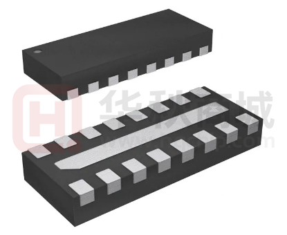
SLP4016P16 16-pin package
RoHS/WEEE Compliant
Nominal Dimensions: 4.0 x 1.6 x 0.58 mm
Lead Pitch: 0.5mm
Lead finish: NiPdAu
Marking: Marking Code
Packaging: Tape and Reel
Applications
T-Flash / MicroSD Interfaces
MMC Interfaces
CDMA, GSM, 3G Cell Phones
The EClamp2410P is in a 16-pin, RoHS/WEEE compliant,
SLP4016P16 package. It measures 4.0 x 1.6 x
0.58mm. The leads are spaced at a pitch of 0.5mm
and are finished with lead-free NiPd.
Package Configuration
Pin Configuration
4.00
DAT1 In
DAT0 In
CLK In
1
16
DAT1 Out
1 2
DAT0 Out
1.60
CLK Out
Rup1
Rup3
Vdd
Rup2
CMD In
CMD Out
DAT3 In
DAT3 Out
DAT2 In
DAT2 Out
0.50 BSC
0.58
Pin Designation (Top View)
Revision 10/26/2007
16 Pin SLP package (Bottom Side View)
Nominal Dimensions in mm
1
�EClamp2410P
PRELIMINARY
PROTECTION PRODUCTS
Pin Identification and Configuration
Pin
Symbol
Identification
1, 16
DAT1
Data line #1 input/output with pull-up resistor
2, 15
DAT0
Data line #0 Input/Output
3, 14
Clock
Clock line Input/Output
4
Rup1
15K Pull-up resistor from DAT1 & DAT2
5
Vdd
Power Supply ESD Protection
6, 11
CMD
Command Line Input/Output
7, 10
DAT3
Data line #3 input/output with pull-up resistor
8, 9
DAT2
Data line #2 input/output with pull-up resistor
12
Rup2
50K Pull-Up Resistor from DAT3
13
Rup3
VCC Circuit 3A
Center tab
GND
Ground connection
16 15 14 13 12 11 10 9
1
2 3 4 5 6 7
Pin Configuration (Top View)
Schematics & Component Values
Pin 1, 8
45 Ohms
Pin 4
Pin 12
Rup
15K
Rup
50K
Pin 7
Pin 9, 16
45 Ohms
DAT1, DAT2
Pin 10
DAT3
DAT0, CMD Line
Pin 13
Rup
15K
Pin 3
45 Ohms
CLK
2007 Semtech Corp.
Pin 14
Pin 5
Vdd
2
Pin 2, 6
45 Ohms
DAT0, CMD
Pin 11, 15
8
�EClamp2410P
PRELIMINARY
PROTECTION PRODUCTS
Maximum Ratings
R ating
Symbol
Value
Units
VESD
+/- 17
+/- 12
kV
Junction Temp erature
TJ
125
o
Op erating Temp erature
Top
-40 to +85
o
Storage Temp erature
TSTG
-55 to +150
o
ESD p er IEC 61000-4-2 (Air)
ESD p er IEC 61000-4-2 (Contact)
C
C
C
Electrical Characteristics (T = 25oC)
P ar am et er
S y m b ol
Con d i t i on s
T VS Reverse Stand-Off Voltage
VRWM
T VS Reverse Breakdown Voltage
V BR
It = 1mA
T VS Reverse Leakage Current
IR
VRWM = 3.0V
Series Resistors
R
Each Line
Mi n i mu m
6
Ty p i c a l
8
M ax i m u m
Units
5
V
10
V
0.5
µA
38
45
52
Ohms
DAT Pull Up Resistor 1
Rup 1
12
15
17
k Ohms
DAT Pull Up Resistor 2
Rup 2
42
50
58
k Ohms
Total Cap acitance
Cin
10
12
15
pF
2007 Semtech Corp.
Inp ut to Gnd,
Each Line
VR = 2.5V, f = 1MHz
3
�EClamp2410P
PRELIMINARY
PROTECTION PRODUCTS
Typical Characteristics
Typical Insertion Loss S21 (Each Line)
CH1 S21
LOG
ESD Clamping
(8kV Contact per IEC 61000-4-2)
6 dB / REF 0 dB
1: -6.145 dB
300 MHz
2: -14.437 dB
900 MHz
0 dB
3: -23.847 dB
1.8 GHz
-6 dB
1
-12 dB
4: -32.024 dB
2.5 GHz
2
-18 dB
-24 dB
3
-30 dB
4
-36 dB
-42 dB
-48 dB
1
MHz
10
MHz
3
1
GHz GHz
100
MHz
STOP 3 000. 000000 MHz
START. 030 MHz
Note: Data is taken with a 10x attenuator
Normalized Capacitance vs. Reverse Voltage
Series Resistance vs. Temperature
50
1.2
f =1MHz
49
Series Resistance (Ohm)
CJ(V R) / CJ(V R=0)
1
0.8
0.6
0.4
0.2
48
47
46
45
44
43
42
41
0
40
0
0.5
1
1.5
2
2.5
3
ReverseVoltage- VR(V)
3.5
4
4.5
-40
5
-10
5
20
35
0
Temperature ( C)
50
65
80
Pull Up Resistance (Rup2) vs. Temperature
16200
58000
16100
57000
16000
56000
Pull Up Resistance (Ohm)
Pull Up Resistance (Ohm)
Pull Up Resistance (Rup1) vs. Temperature
-25
15900
15800
15700
15600
15500
15400
15300
55000
54000
53000
52000
51000
50000
49000
15200
-40
-30
-20
-10
0
10
20
30
o
40
50
60
70
48000
80
-40
Temperature ( C)
2007 Semtech Corp.
-30
-20
-10
0
10
20
30
o
40
Temperature ( C)
4
50
60
70
80
�EClamp2410P
PRELIMINARY
PROTECTION PRODUCTS
Applications Information
Device Connection
Figure 1 - Pin Identification and Configuration
(Top Side View)
The EClamp2410P is a microSD/T-Flash interface device
designed for use in cell phones and other portable
electronic devices. The EClamp2410P is comprised of
series and pull up resistors required on the microSD
interface. Each line also includes TVS diodes for ESD
protection. The device may be configured for SD or SPI
mode operation. In SD mode for example, the 15k Ohm
pull up resistors (Rup 1 and Rup 3) are connected to
VDD. In SPI mode pin 4 is not connected (Rup 1) since
these are reserved lines. The 50k Ohm pull up resistor is
used for card detection or SPI mode selection during
power up and is disconnected by the user during regular
data transfer.
The EClamp2410P is in a 16-pin SLP package. Electrical
connection is made to the 16 pins located at the bottom
of the device. The device has a flow through design for
easy layout. Pin connections are noted in Figure 1. A
center tab serves as the ground connection. Recommendations for the ground connection are given below.
Ground Connection Recommendation
Parasitic inductance present in the board layout will
affect the filtering and ESD performance of the device.
Ground loop inductance can be reduced by using multiple vias to make the connection to the ground plane.
Figure 2 shows the recommended device layout. The
ground pad vias have a diameter of 0.008 inches (0.20
mm) while the two external vias have a diameter of
0.010 inches (0.250mm). The internal vias are spaced
approximately evenly from the center of the pad. The
designer may choose to use more vias with a smaller
diameter (such as 0.005 inches or 0.125mm) since
changing the diameter of the via will result in little
change in inductance.
DAT1 In
DAT0 In
CLK In
16
DAT1 Out
DAT0 Out
CLK Out
Rup1
Rup3
Vdd
Rup2
CMD In
CMD Out
DAT3 In
DAT3 Out
DAT2 In
DAT2 Out
Figure 2 - Recommended Layout using Ground Vias
The ESD transient return path to ground should
be kept as short as possible. Whenever possible, use
multiple micro vias connected directly from the
device ground pad to the ground plane.
Avoid running critical signals near board edges.
Layout Guidelines for Optimum ESD Protection
Good circuit board layout is critical not only for signal
integrity, but also for effective suppression of ESD
induced transients. For optimum ESD protection, the
following guidelines are recommended:
Place the device as close to the connector as
possible. This practice restricts ESD coupling into
adjacent traces and reduces parasitic inductance.
2007 Semtech Corp.
1
5
�EClamp2410P
PRELIMINARY
MicroSD Connector
PROTECTION PRODUCTS
Applications Information
DAT 1 IN
DAT 1 OUT
DAT 0 IN
DAT 0 OUT
CLK IN
CLK OUT
Rup 15KΩ
Rup 15KΩ
VDD
Rup 50KΩ
CMD IN
CMD OUT
DAT 3 IN
DAT 3 OUT
DAT 2 IN
DAT 2 OUT
EClamp2410P
Figure 3 - MicroSD Protection
2007 Semtech Corp.
6
Host IC
�EClamp2410P
PRELIMINARY
PROTECTION PRODUCTS
Applications Information - Spice Model
Pin 12
Pin 4, 13
Rup
50K
Rup
15K
Pin 1, 8, 2, 6
45 Ohms
D1
Pin 7
Pin 9, 16, 11, 15
45 Ohms
Pin 10
D1
D1
D1
DAT3
DAT1, DAT2, DAT0, CMD
Pin 5
Pin 3
45 Ohms
Pin 14
D1
D1
D1
CLK
Vdd
EClamp2410P Spice Model
EClamp2410P Spice Parameters
2007 Semtech Corp.
Parameter
Unit
D1 (T VS)
IS
A mp
2E-15
BV
Volt
7.46
VJ
Volt
0.777
RS
Ohm
1.00
IB V
Amp
1E-3
CJO
Farad
10E-12
TT
sec
2.541E-9
M
--
0.246
N
--
1.1
EG
eV
1.11
7
�EClamp2410P
PRELIMINARY
PROTECTION PRODUCTS
Outline Drawing - SLP4016P16
A
B
D
DIM
E
PIN 1
INDICATOR
(LASER MARK)
A
SEATING
PLANE
aaa C
A2
C
A1
D1
A
A1
A2
b
D
D1
E
E1
e
L
N
aaa
bbb
DIMENSIONS
INCHES
MILLIMETERS
MIN NOM MAX MIN NOM MAX
.020 .023 .026 0.50 0.58 0.65
.000 .001 .002 0.00 .003 0.05
(0.13)
(.005)
.007 .010 .012 0.20 0.25 0.30
.153 .157 .161 3.90 4.00 4.10
.122 .126 .130 3.10 3.20 3.30
.059 .063 .067 1.50 1.60 1.70
.010 .016 .020 0.25 0.40 0.50
0.50 BSC
.020 BSC
.011 .013 .015 0.28 0.33 0.38
16
16
0.08
.003
0.10
.004
1 2
LxN
E/2
E1
N
bxN
e
bbb
C A B
D/2
NOTES:
1. CONTROLLING DIMENSIONS ARE IN MILLIMETERS (ANGLES IN DEGREES).
2. COPLANARITY APPLIES TO THE EXPOSED PAD AS WELL AS THE TERMINALS.
Land Pattern - SLP4016P16
P
X
Z
F
G
Y
(C)
DIM
B
C
F
G
P
X
Y
Z
DIMENSIONS
INCHES
MILLIMETERS
.130
3.30
.060
1.52
.018
0.45
.035
0.89
.020
0.50
.012
0.30
.025
0.63
.085
2.15
B
NOTES:
1. THIS LAND PATTERN IS FOR REFERENCE PURPOSES ONLY.
CONSULT YOUR MANUFACTURING GROUP TO ENSURE YOUR
COMPANY'S MANUFACTURING GUIDELINES ARE MET
2007 Semtech Corp.
8
�EClamp2410P
PRELIMINARY
PROTECTION PRODUCTS
Marking
Ordering Information
2410P
YX
PIN 1
INDICATOR
(LASER MARK)
Part Number
Qty per
Reel
Reel Size
EClamp2410P.TCT
3000
7 Inch
EMIClamp and EClamp are marks of Semtech Corporation
Tape and Reel Specification
Pin 1 Location
User Direction of feed
Device Orientation in Tape
A0
1.78 +/-0.10 mm
B0
K0
4.30 +/-0.10 mm
0.74 +/-0.10 mm
Tape
Width
B, (Max)
D
D1
12 mm
8.2 mm
(.476)
1.5 + 0.1 mm
- 0.0 mm
(0.59 +.005
- .000)
1.0 mm
±0.05
(.039)
2007 Semtech Corp.
E
1.750±.10
mm
(.069±.004)
F
K
(MAX)
P
P0
P2
T(MAX)
W
5.5±0.05
mm
(.217±.002)
4.5 mm
(.177)
4.0±0.1
mm
(.157±.004)
4.0±0.1
mm
(.157±.004)
2.0±0.05mm
(.079±.002)
0.4 mm
(.016)
12.0 mm
+ 0.3 mm
- 0.1 mm
(.472±.012)
9
�
很抱歉,暂时无法提供与“ECLAMP2410P.TCT”相匹配的价格&库存,您可以联系我们找货
免费人工找货- 国内价格
- 5+13.34221
- 750+12.94857
- 1500+12.55493
- 国内价格
- 1+8.77500
- 10+8.45000
- 100+7.67000
- 500+7.28000
- 国内价格 香港价格
- 1+22.262231+2.87083
- 10+14.2653910+1.83960
- 100+9.68552100+1.24900
- 500+7.72334500+0.99597
- 1000+7.092161000+0.91457
- 国内价格
- 1+18.15865
- 10+12.33734
- 50+9.75009
- 100+8.76790
- 125+8.49240
- 500+7.06702
- 1000+6.79153