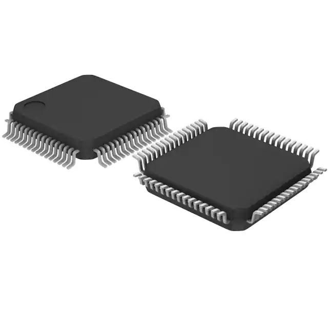
GS1535 HD-LINX II™ Multi-Rate SDI Automatic Reclocker
GS1535 Data Sheet Key Features • • • • • • • • • • • • • • • SMPTE 292M, 259M and 344M compliant Supports data rates of 143, 177, 270, 360, 540, 1483.5, 1485 Mb/s Supports DVB-ASI at 270Mb/s Auto and Manual Modes for rate selection Standards indication in Auto Mode 4:1 input multiplexor Lock Detect Output On-chip Input and Output Termination Differential inputs and outputs Configuarble automatic Mute or Bypass when not locked Manual Bypass function SD/HD indication output to control GS1528 Dual Slew-Rate Cable Driver Pb-free and Green Single 3.3V power supply Operating temperature range: 0°C to 70°C Description The GS1535 Multi-Rate Serial Digital Reclocker is designed to automatically recover the embedded clock signal and re-time the data from a SMPTE 292M, SMPTE 259M or SMPTE 344M compliant digital video signal. The device removes the high frequency jitter components from the bit-serial stream. Input termination is on-chip for seamless matching to 50Ω transmission lines. An LVPECL compliant output interfaces seamlessly to the GS1528 Cable Driver The GS1535 can operate in either auto or manual rate selection mode. In Auto mode the GS1535 automatically detects and locks onto an incoming SMPTE SDI data signal from 143 Mb/s to 1.485 Gb/s. For single rate data systems, the GS1535 can be configured to operate in manual mode. In both modes, the GS1535 requires only one external crystal to set the VCO frequency when not locked and provides adjustment free operation. In systems which require passing non-SMPTE data rates, the GS1535 will automatically or manually enter a bypass mode in order to pass the signal without reclocking. The ASI/177 input pin allows for manual selection of support of either 177Mb/s or DVB-ASI inputs.
Applications • SMPTE 292M, SMPTE 259M and SMPTE 344M Serial Digital Interfaces
XTAL+ XTAL-
XTAL XTAL OUT+ OUT-
LF+ LF-
KBB
XTAL OSC
BUFFER
RE-TIMER
M U X
DATA BUFFER
DDO/DDO
DDO_MUTE DDI 0
PHASE FREQUENCY DETECTOR D A T A M U X
M U X
CHARGE PUMP
VCO
DDI 1
PHASE DETECTOR DIVIDE BY 2,4,6,8,12,16 DIVIDE BY 152, 160, 208
DDI 2
DDI 3
DDI_SEL[1:0]
CONTROL LOGIC
BYPASS LOGIC
SS[2:0]
ASI/177
AUTO/MAN
LD
AUTOBYPASS
BYPASS
GS1535 Functional Block Diagram
18557 - 8 February 2005 1 of 22 www.gennum.com
�GS1535 Data Sheet
Contents
Key Features .................................................................................................................1 Applications...................................................................................................................1 Description ....................................................................................................................1 1. Pin Out ......................................................................................................................3 1.1 Pin Assignment ...............................................................................................3 1.2 Pin Descriptions ..............................................................................................4 2. Electrical Characteristics ...........................................................................................7 2.1 Absolute Maximum Ratings ............................................................................7 2.2 DC Electrical Characteristics ..........................................................................7 2.3 AC Electrical Characteristics ...........................................................................8 2.4 Input/Output Circuits .....................................................................................10 3. Detailed Description ................................................................................................13 3.1 Slew Rate Phase Lock Loop (S-PLL) ...........................................................13 3.2 VCO ..............................................................................................................14 3.3 Charge Pump ................................................................................................14 3.4 Frequency Acquisition Loop —The Phase-Frequency Detector ...................14 3.5 Phase Acquisition Loop — The Phase Detector ...........................................15 3.6 4:1 Input Mux ................................................................................................15 3.7 Automatic And Manual Data Rate Selection .................................................16 3.8 Bypass Mode ................................................................................................17 3.9 DVB/ASI Operation .......................................................................................17 3.10 LOCK ..........................................................................................................17 3.11 Output Drivers .............................................................................................18 3.12 Output Mute ................................................................................................18 4. Application Reference Design .................................................................................19 4.1 Typical Application Circuit .............................................................................19 5. References ..............................................................................................................20 6. Package & Ordering Information .............................................................................20 6.1 Package Dimensions ....................................................................................20 6.2 Packaging Data .............................................................................................21 6.3 Ordering Information .....................................................................................21 7. Revision History ......................................................................................................22
18557 - 8
February 2005
2 of 22
�GS1535 Data Sheet
1. Pin Out
1.1 Pin Assignment
XTAL_OUT+ 50 XTAL_OUTVCC_CP
VEE_CP
XTAL+
RSVD
XTAL-
RSVD
RSVD
GND
GND
64
63
62
61
60
59
58
57
56
55
54
53
52
51
49 VEE_DDO VCC_DDO DDO DDO_VTT DDO GND VEE_INT VCC_INT RSVD RSVD RSVD GND DDO_MUTE GND KBB SD/HD
DDI0 DDI0_VTT DDI0 GND DDI1 DDI1_VTT DDI1 GND DDI2 DDI2_VTT DDI2 GND DDI3 DDI3_VTT DDI3 GND
1 2 3 4 5 6 7 8 9 10 11 12 P 13 14 15 16 GS1535 64 PIN LQFP TOP VIEW
GND 48 47 46 45 44 43 42 41 40 39 38 37 36 35 34 33 32 GND
17 DDI_SEL0
18 DDI_SEL1
19 BYPASS
20 AUTOBYPASS
21 AUTO/MAN
22 VCC_VCO
23 VEE_VCO
24 SS0
25 SS1
26 SS2
VCC
VCC
LF+
LF-
27 ASI/177
28 LD
29 RSVD
30 VCC_DIG
31 VEE_DIG
18557 - 8
February 2005
3 of 22
�GS1535 Data Sheet
1.2 Pin Descriptions
Table 1-1: Pin Descriptions Pin Number
1, 3 2 5, 7 6 9, 11 10 13, 15 14 17, 18
Name
DDI0, DDI0 DDI0_VTT DDI1,DDI1 DDI1_VTT DDI2, DDI2 DDI2_VTT DDI3, DDI3 DDI3_VTT DDI_SEL[1:0]
Type
INPUT PASSIVE INPUT PASSIVE INPUT PASSIVE INPUT PASSIVE LOGIC INPUT
Description
Serial digital differential input 0. Center tap of two 50Ω on-chip termination resistors between DDI0 and DDI0. Serial digital differential input 1. Center tap of two 50Ω on-chip termination resistors between DDI1 and DDI1. Serial digital differential input 2. Center tap of two 50Ω on-chip termination resistors between DDI2 and DDI2. Serial digital differential input 3 . Center tap of two 50Ω on-chip termination resistors between DDI3 and DDI3. Serial digital input select. DDI_SEL1 0 0 1 1 DDI_SEL0 0 1 0 1 INPUT SELECTED DDI0 DDI1 DDI2 DDI3
19 20
BYPASS AUTOBYPASS
LOGIC INPUT LOGIC INPUT
Bypasses the reclocker stage (Active HIGH). When BYPASS is HIGH, it overwrites the AUTOBYPASS setting. Automatically bypasses the reclocker stage when the PLL is not locked (Active HIGH).
21
AUTO/MAN
LOGIC INPUT
When active, the standard is automatically detected from the input data rate.
18557 - 8
February 2005
4 of 22
�GS1535 Data Sheet
Table 1-1: Pin Descriptions (Continued) Pin Number
24, 25, 26
Name
SS[2:0]
Type
BIDIRECTIONAL
Description
When AUTO/MAN is HIGH, SS[0:2] are outputs, displaying the data rate to which the PLL has locked. When AUTO/MAN is LOW, SS[0:2] are inputs, forcing the PLL to lock only to a selected data rate. SS2 0 0 0 0 1 1 SS1 0 0 1 1 0 0 SS0 0 1 0 1 0 1 DATA RATE SELECTED/FORCED (Mb/s) 143 177 270 360 540 1483.5/1485
27 28 29 33
ASI/177 LD RSVD SD/HD
LOGIC INPUT OUTPUT RESERVED OUTPUT
Disables 177Mbps data rate in the AUTO data rate detection circuit. This prevents a FALSE LOCK to 177Mbps when using DVB/ASI. LOCK DETECT. HIGH when the PLL is locked. DO NOT CONNECT. This signal is LOW when the reclocker has locked to 1.485Gbps or 1.485/1.001Gbps, and HIGH when the reclocker has locked to 143Mbps, 177Mbps, 270Mbps, 360Mbps, or 540Mbps. Controls the loop bandwidth of the PLL. Leave this pin floating for serial reclocking applications. Mutes the DDO/DDO outputs, when not in bypass mode. Differential Serial Digital Outputs. Center tap of two 50Ω on-chip termination resistors between DDO and DDO.. Differential buffered outputs of the reference oscillator. Reference crystal input. Connect to the GO1535. Loop filter capacitor connection. (CLF = 47nF). Recommended connect to GND.
34 36 44, 46 45 50, 51 52, 53 62, 63 4, 8, 12,16, 32, 35, 37, 43, 49, 54, 64 43
KBB DDO_MUTE DDO, DDO DDO_VTT XTAL_OUT+, XTAL_OUTXTAL+, XTALLF+, LFGND
ANALOG INPUT LOGIC INPUT OUTPUT PASSIVE OUTPUT INPUT PASSIVE PASSIVE
GND_DRV
PASSIVE
Recommended connect to GND.
18557 - 8
February 2005
5 of 22
�GS1535 Data Sheet
Table 1-1: Pin Descriptions (Continued) Pin Number
55, 57 22 30 41 47 61 23 31 42 48 60 38, 39, 40, 56, 58, 59
Name
VCC VCC_VCO VCC_DIG VCC_INT VCC_DDO VCC_CP VEE_VCO VEE_DIG VEE_INT VEE_DDO VEE_CP RSVD
Type
PASSIVE POWER POWER POWER POWER POWER POWER POWER POWER POWER POWER RESERVED
Description
Recommend connect to 3.3V. Most positive power supply connection for the internal VCO section. Connect to 3.3V. Most positive power supply connection for the internal glue logic. Connect to 3.3V. Most positive power supply connection. Connect to 3.3V. Most positive power supply connection for the DDO/DDO output driver. Connect to 3.3V. Most positive power supply connection for the internal charge pump. Connect to 3.3V. Most negative power supply connection for the internal VCO section. Connect to ground. Most negative power supply connection for the internal glue logic. Connect to ground. Most negative power supply connection. Connect to ground. Most negative power supply connection for the DDO/DDO output driver. Connect to ground. Most negative power supply connection for the internal charge pump. Connect to ground. Do not Connect.
18557 - 8
February 2005
6 of 22
�GS1535 Data Sheet
2. Electrical Characteristics
2.1 Absolute Maximum Ratings
Table 2-1: Absolute Maximum Ratings Parameter
Supply Voltage Input ESD Voltage Storage Temperature Range Inputs
Value
+3.6 VDC 500V -50°C< Ts < 125°C VCC + 0.5V
2.2 DC Electrical Characteristics
Table 2-2: DC Electrical Characteristics
Vcc = 3.3V, TA = 0°C to 70°C, unless otherwise shown
Parameter
Supply Voltage Power Consumption Supply Current Logic Inputs DDI_SEL[1:0], BYPASS, AUTOBYPASS, AUTO/MAN, ASI/177, SDO_MUTE Logic Outputs SD/HD and LD
Conditions
Operating Range TA=25°C TA=25°C High Low
Symbol
VCC
Min
3.135 408
Typ
3.3 600 182 -
Max
3.465 849 245 0.8
Units
V mW mA V V
Test Levels
3 5 1 3 3
ICC VIH VIL
130 2.0 -
250µA Load
VOH VOL
3.2 2.0 -
-
0.6 0.8
V V V V
3 3 3 3
Bi-Directional Pins SS[2:0], AUTO/MAN = 0 (Manual Mode) Bi-Directional Pins SS[2:0], AUTO/MAN = 1 (AUTO Mode)
High Low
VIH VIL
High Low
VOH VOL
2.6 -
0.6
V V
1 1
18557 - 8
February 2005
7 of 22
�GS1535 Data Sheet
Table 2-2: DC Electrical Characteristics
Vcc = 3.3V, TA = 0°C to 70°C, unless otherwise shown
Parameter
XTAL_OUT+, XTAL_OUT-
Conditions
High Low
Symbol
VOH VOL
Min
1.65 + (VSID/2) -
Typ
VCC VCC - 0.285 -
Max
VCC - (VSID/2) -
Units
V V V
Test Levels
7 7 1
Serial Input Voltage Output Voltage SDO, SDO Test Levels
Common mode Common mode
VCC - VOD/2
V
1
1. Production test at room temperature and nominal supply voltage with guardbands for supply and temperature ranges. 2. Production test at room temperature and nominal supply voltage with guardbands for supply and temperature ranges using correlated test. 3. Production test at room temperature and nominal supply voltage. 4. QA sample test. 5. Calculated result based on Level 1, 2, or 3. 6. Not tested. Guaranteed by design simulations. 7. Not tested. Based on characterization of nominal parts. 8. Not tested. Based on existing design/characterization data of similar product. 9. Indirect test.
2.3 AC Electrical Characteristics
Table 2-3: AC Electrical Characteristics
Vcc = 3.3V, TA = 0°C to 70°C, unless otherwise shown
Parameter
Serial Input Data Rate Serial Input Jitter Tolerance
Symbol
Conditions
Min
143
Typ
-
Max
1485 -
Units
Mb/s UI
Test Levels
3 1
Worst case modulation Eg. Square wave modulation 143, 270, 360, 1485 Mb/s
0.8
PLL Lock Time Asynchronous PLL Lock Time - Synchronous
t ALOCK t SLOCK CLF=47nF SD/HD=0 SD/HD=1
0.29 0.16 50Ω load (on chip) Differential (across 100Ω). 100 1400
5 114 106 -
10 800 2000
ms µs µs ps ps mVp-p mVp-p
6,7 6,7 6,7 6,7
Serial Output Rise/Fall Time (20% - 80%)
trSDO tfSDO
50Ω load (on chip)
Serial Input - Signal Swing Serial Output - Signal Swing
VSID
6,7
VOD
18557 - 8
February 2005
8 of 22
�GS1535 Data Sheet
Table 2-3: AC Electrical Characteristics
Vcc = 3.3V, TA = 0°C to 70°C, unless otherwise shown
Parameter
Serial Output Jitter (additive)
Symbol
tIJ
Conditions
KBB=Float, PRN, 223 -1 143Mb/s 177Mbs 270Mb/s 360Mbs 540Mbs 1485Mb/s BYPASS
Min
0.25UI), Q-clk will sample a different value than I-clk. In this condition, two extra phase correction signals will be generated which instructs the charge pump to create larger frequency corrections for the VCO.
i-PHASE ALIGNMENT EDGE DATA RE-TIMING EDGE
I-clk
q-clk
q-PHASE ALIGNMENT EDGE
INPUT DATA WITH JITTER
0.25UI 0.8UI
RE-TIMED OUTPUT DATA
Figure 3-2: Phase Detector Characteristics.
When the PA loop is active, the crystal frequency and the incomming data rate are compared. If the resultant is more that 2%, the PLL is considered to be unlocked and the system jumps to the FA loop.
3.6 4:1 Input Mux
The 4:1 input mux allows the connection of four independent streams of video/data. These are differential inputs (DDI[3:0] and DDI[3:0]). The active channel can be selected via the DDI_SEL[1:0] pins. Table 3-1 shows the input selected for a given state at DDI_SEL[1:0].
Table 3-1: Bit Pattern for Input Select DDI_SEL1:0]
00 01 10 11
Selected Input
DDI0 DDI1 DDI2 DDI3
18557 - 8
February 2005
15 of 22
�GS1535 Data Sheet The DDI inputs are designed to be DC interfaced with the output of the GS1524 Cable Equalizer. There are on chip 50Ω termination resistors which come to a common point at the DDI_VT pins. Connect a 10nF capacitor to this pin and connect the other end of the capacitor to ground. This end-terminates the transmission line at the inputs for optimum performance. If only one input pair is used, connect the unused positive inputs to +3.3V and leave the unused negative inputs floating. This helps to eliminate crosstalk from potential noise that would couple to the unused input pair.
3.7 Automatic And Manual Data Rate Selection
The GS1535 can be configured to manually lock to a specific data rate or automatically search for and lock to the incoming data rate. The AUTO_MAN pin selects Automatic data rate detection mode (AUTO mode) when HIGH and manual data rate selection mode (MANUAL mode) when LOW. In AUTO mode, the SS[2:0] bi-directional pins become outputs and the bit pattern indicates the data rate that the PLL is locked to (or previously locked to). The "search algorithm" cycles through the data rates (see Figure 3-3) and starts over if that data rate is not found.
POWER-UP
143 Mb\s
177 Mb\s
270Mb\s
360 Mb\s
1.485Mb\s
540 Mb\s
Figure 3-3: Data Rate Search Pattern
NOTE: When the device is in AUTO mode, the SD/HD output will toggle when the reclocker is not locked, (LD=LOW). The logic level of SD/HD will depend on the current state of the search algorithm. If the device is also in bypass mode, and the SD/HD signal is used to set the slew rate of the GS1528 Cable Driver, that slew rate will change dynamically when the reclocker is not locked. In MANUAL mode, the SS[2:0] pins become inputs and the data rate can be programmed. In this mode, the search algorithm is disabled and the GS1535's PLL will only lock to this data rate. Table 3-2 shows the bit pattern at SS[2:0] for the data rate selected (in MANUAL mode) or the data rate that the PLL has locked to (in AUTO mode).
18557 - 8
February 2005
16 of 22
�GS1535 Data Sheet
Table 3-2: Data Rate Indication/Selection Bit Pattern SS[2:0]
000 001 010 011 100 101
Data Rate (Mb/s)
143 177 270 360 540 1485/1483.5
3.8 Bypass Mode
In bypass mode, the GS1535 passes the data at the inputs, directly to the outputs. There are two pins that control the bypass function: BYPASS and AUTOBYPASS. The BYPASS pin is an active high signal which forces the GS1535 into bypass mode for as long as a HIGH is asserted at this pin. The AUTOBYPASS pin is an active high signal which places the GS1535 into bypass mode only when the PLL has not locked to a data rate. Note that if BYPASS is HIGH, this will overwrite the AUTOBYPASS functionallity. When the GS1535’s PLL is not locked and BYPASS = LOW and AUTOBYPASS = LOW, the serial digital output DDO/DDO will produce invalid data.
3.9 DVB/ASI Operation
The GS1535 is designed to re-clock DVB/ASI at 270 Mb/s. There is a harmonic present in idle patterns (K28.5) which is very close the 177 Mb/s data rate (EIC 1179). The ASI/177 pin, when HIGH will disable the 177 Mb/s search in AUTO mode. In this mode, the GS1535 will not lock to 177 Mb/s.
3.10 LOCK
The LOCK DETECT signal, LD, is an active high output which indicates when the PLL is locked. The lock logic with the GS1535 includes a system which monitors the Frequency Acquisition Loop and the Phase Acquisition Loop as well as a monitor to detect harmonic lock.
18557 - 8
February 2005
17 of 22
�GS1535 Data Sheet
3.11 Output Drivers
The GS1535’s serial digital data outputs (DDO/DDO) have a nominal voltage of 800mv single ended or 1600mV differential when terminated into 50Ω. The DDO_VTT pin is the common point of two 50Ω termination resistors from the DDO and DDO. This pin can be left open if the termination exists on the receiving device.
3.12 Output Mute
The DDO_MUTE pin is provided to allow muting of the retimed output. When the GS1535’s PLL is locked and the device is reclocking, setting DDO_MUTE = LOW will force the serial digital outputs DDO/DDO to mute. However, if the GS1535 is in bypass mode, (AUTOBYPASS = HIGH and/or BYPASS = HIGH), DDO_MUTE will have no effect on the output.
18557 - 8
February 2005
18 of 22
�GS1535 Data Sheet
4. Application Reference Design
4.1 Typical Application Circuit
GO1535 (14.140MHz) 47n
3.3V
3.3V 56
10n
GND 64
63
62
61
60 59
58
57
56
55
54
53
52 51
50 XTAL_OUT+ XTAL_OUT-
VCC_CP
RSVD
RSVD
VCC
LF+
XTAL+
VCC
RSVD
GND
VEE_CP
XTAL-
GND
LF-
49
1
DDI0 DDI0_VT DDI0 GND DDI1 DDI1_VT DDI1 GND DDI2 DDI2_VT DDI2 GND DDI3 DDI3_VT DDI3
VEE_DDO VCC_DDO DDO DDO_VTT DDO GND VEE_INT
48 1 0n 47 46 45 44 43 42 1 0n 41 40 3.3V 65 3.3V
D ATA I N P U T 0
Zo = 50
2 10n 3 4 5
Zo = 50
10n
D ATA O U T P U T
D ATA I N P U T 1
Zo = 50
6 10n 7 8 9
GS1535
VCC_INT RSVD RSVD RSVD GND DDO_MUTE GND KBB
D ATA I N P U T 2
Zo = 50
10 10n 11 12 13
39 38 37 36 35 34 SDO_MUTE
D ATA I N P U T 3
Zo = 50
14 10n 15 16
AUTOBYPASS
AUTO/MAN
GND
SD/HD
33
SD/HD
VCC_VCO
DDI_SEL0
DDI_SEL1
VCC_DIG
VEE_VC0
VEE_DIG 31
3.3V
BYPASS
ASI/177
RSVD
17
18
19
20
21
22
23
24
25
26
27
28
29
30
10n DDI_SEL0 DDI_SEL1 ASI_177 3.3V
10n
32
GND
SS0
SS1
SS2
LD
LD
Note: All resistors in ohms and all capacitors in Farads.
Figure 4-1: Typical Application Circuit
18557 - 8
February 2005
19 of 22
�GS1535 Data Sheet
5. References
Compliant with SMPTE 292M, SMPTE 259M and SMPTE344M.
6. Package & Ordering Information
6.1 Package Dimensions
Table X
0 0 0 0
NOTE: Diagram shown is representative only. Table X is fixed for all pin sizes, and Table Y is specific to the 64-pin package.
Table Y
SYMBOL M I L L I M E TE R MIN b e D2 E2 0.17 NOM 0.20 MAX 0.27 MIN 64L INCH NOM M AX
0.007 0.008 0.011 0.020 BSC 0.295 0.295
0.50 BSC 7.50 7.50
TOLERANCES OF FORM AND POSITION aaa bbb ccc 0.20 0.20 0.08 0.008 0.008 0.003
18557 - 8
February 2005
20 of 22
�GS1535 Data Sheet
6.2 Packaging Data
Parameter
Package Type Package Drawing Reference Moisture Saturation Level Junction to Case Thermal Resistance, θj-c Junction to Air Thermal Resistance, θj-a (at zero airflow) Psi Pb-free and Green
Value
10mm x 10mm 64-pin LQFP JEDEC MS026 3 14.9°C/W 45.4°C/W 0.9°C/W Yes
6.3 Ordering Information
Part Number
GS1535-CFU GS1535-CFUE3
Package
64 pin LQFP 64 pin LQFP
Temperature Range
0°C to 70°C 0°C to 70°C
Pb-Free And Green
No Yes
18557 - 8
February 2005
21 of 22
�GS1535 Data Sheet
7. Revision History
Version
7
ECR
134667
Date
November 2004
Changes and / or Modifications
Corrected TAC pinout for pins 50, 51. Added packaging data section. Updated pins 62 and 63 on the typical application circuit. Converted to new document template. Corrected block diagram and pin description table to reflect mute functionality of the device.
8
135363
January 2005
CAUTION
ELECTROSTATIC SENSITIVE DEVICES DO NOT OPEN PACKAGES OR HANDLE EXCEPT AT A STATIC-FREE WORKSTATION DOCUMENT IDENTIFICATION
DATA SHEET
The product is in production. Gennum reserves the right to make changes to the product at any time without notice to improve reliability, function or design, in order to provide the best product possible.
GENNUM CORPORATION
Mailing Address: P.O. Box 489, Stn. A, Burlington, Ontario, Canada L7R 3Y3 Shipping Address: 970 Fraser Drive, Burlington, Ontario, Canada L7L 5P5 Tel. +1 (905) 632-2996 Fax. +1 (905) 632-5946
GENNUM JAPAN CORPORATION
Shinjuku Green Tower Building 27F, 6-14-1, Nishi Shinjuku, Shinjuku-ku, Tokyo, 160-0023 Japan Tel. +81 (03) 3349-5501, Fax. +81 (03) 3349-5505
GENNUM UK LIMITED
25 Long Garden Walk, Farnham, Surrey, England GU9 7HX Tel. +44 (0)1252 747 000 Fax +44 (0)1252 726 523 Gennum Corporation assumes no liability for any errors or omissions in this document, or for the use of the circuits or devices described herein. The sale of the circuit or device described herein does not imply any patent license, and Gennum makes no representation that the circuit or device is free from patent infringement. GENNUM and the G logo are registered trademarks of Gennum Corporation. © Copyright 2002 Gennum Corporation. All rights reserved. Printed in Canada. www.gennum.com
18557 - 8
February 2005 22
22 of 22
�